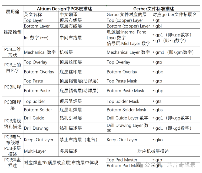
Today, while preparing to prototype a PCB, I suddenly wanted to see what the GCode files we usually use look like, so I downloaded a Gerber file viewer.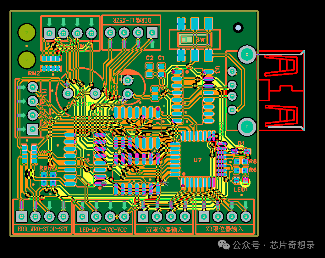 Typically, a Gerber compressed package contains the following files, which can be referenced for the variations.
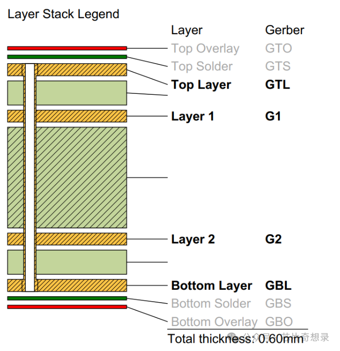 The contents of the corresponding folder are as follows:
 The Gerber files exported from JLCPCB are slightly different, with the following unique files: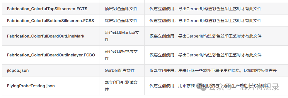
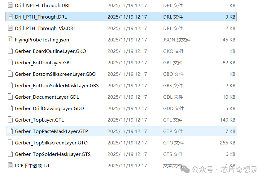 * Not necessarily one-to-one correspondence.
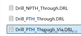 Drill refers to the drilling file, Via refers to the via file, but PTH may also have via data without a Via. After opening, you can see the G-Code format file. G-Code format is often used in CNC machines, 3D printers, and other devices, using letters and numbers to describe the type of operation and the target of the operation.
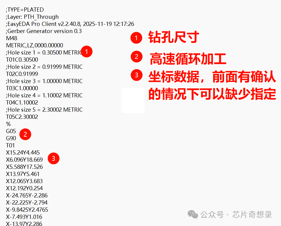 * I will place a commonly used Chinese translation version of G-Code at the end, but strangely, it seems that complete translated documents for G-Code are quite rare. If any experts have them, could you please share? Thank you.
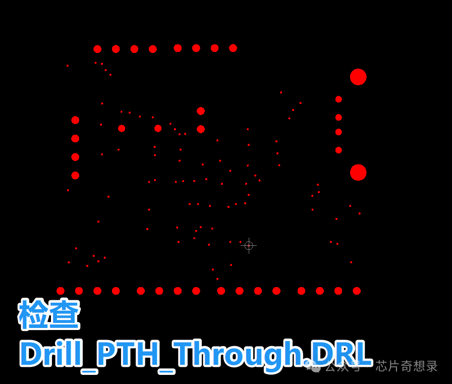 Taking the drilling file as an example, if the data group under T1 is deleted while keeping other drilling files, will it look different when opened? After modification, open:
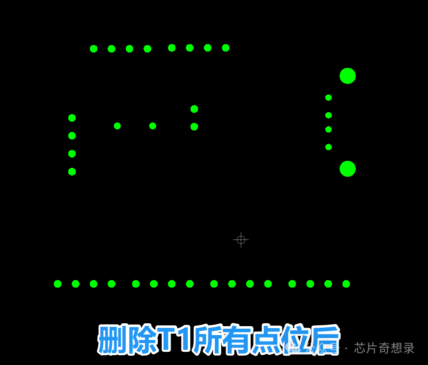 It can be seen that the relevant data has been filtered out. However, the data for the silkscreen layer is also different from the above, which only requires drilling.
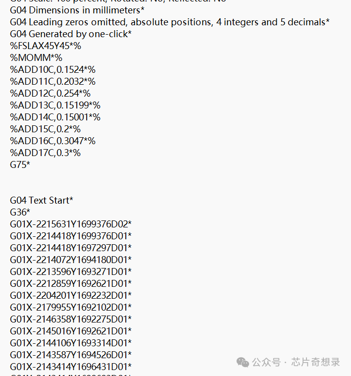 Here, G01 indicates the XY coordinates. This format is similar for the top layer routing and the silkscreen layer. The various files and layers can be referenced in this table:
| Gerber_BoardOutline.GKO | Outline File | The PCB manufacturer uses this file to cut the board shape. The slot area drawn in JLCPCB EDA is reflected in the outline file after generating Gerber. |
| Gerber_TopLayer.GTL | PCB Top Layer | Top copper foil layer |
| Gerber_BottomLayer.GBL | PCB Bottom Layer | Bottom copper foil layer |
| Gerber_InnerLayer1.G1 | Inner Copper Foil Layer | Signal layer type |
| Gerber_InnerLayer2.G2 | Inner Copper Foil Layer | Inner layer of inner power layer, output as positive film, drawn as negative film during PCB drawing (the drawn lines are not output in Gerber). Note: Versions V2.2.33 and earlier used GP+ numeric suffix to indicate inner power layer, later changed to G+ numeric method to avoid conflicts with other EDA negative film inner layer suffixes. |
| Gerber_TopSilkLayer.GTO | Top Silkscreen Layer | Used for top silkscreen patterns and files |
| Gerber_BottomSilkLayer.GBO | Bottom Silkscreen Layer | Used for bottom silkscreen patterns and files |
| Gerber_TopSolderMaskLayer.GTS | Top Solder Mask Layer | Also known as window layer, the default board is covered with solder mask, elements drawn in this layer corresponding to the top area will not be covered with solder mask |
| Gerber_BottomSolderMaskLayer.GBS | Bottom Solder Mask | Also known as window layer, the default board is covered with solder mask, elements drawn in this layer corresponding to the bottom area will not be covered with solder mask |
| Gerber_TopPasteMaskLayer.GTP | Top Paste Mask Layer | For stencil opening |
| Gerber_BottomPasteMaskLayer.GBP | Bottom Paste Mask Layer | For stencil opening |
| Gerber_TopAssemblyLayer.GTA | Top Assembly Layer | For reading only, does not affect PCB manufacturing |
| Gerber_BottomAssemblyLayer.GBA | Bottom Assembly Layer | For reading only, does not affect PCB manufacturing |
| Gerber_MechanicalLayer.GME | Mechanical Layer | Records information in the mechanical layer of PCB design, used only for information recording, this layer’s shape is not used in production, it is only for text identification. For example: process parameters, V-cut paths, etc. |
| Gerber_DocumentLayer.GDL | Document Layer | Used to record PCB notes, does not participate in manufacturing |
| Gerber_CustomLayer1.GCL | User Defined Layer | User-defined layers generally do not belong to the layers required for generation. If production is needed, communication with the board factory is necessary. |
| Gerber_DrillDrawingLayer.GDD | Drilling Layer | This layer does not participate in manufacturing, used for reference marking of the generated via positions |
| Gerber_TopStiffenerLayer_xx_xx.GTSL | Top Stiffener Layer | Used only by JLCPCB, this file is the stiffener layer, xx indicates the stiffener type parameters |
| Gerber_BottomStiffenerLayer_xx_xx.GBSL | Bottom Stiffener Layer | Used only by JLCPCB, this file is the stiffener layer, xx indicates the stiffener type parameters |
| Drill_PTH_Through.DRL | Drilling Layer for Metalized Through Holes | This file shows the positions of holes that need to be metalized on the inner wall, such as multilayer pads and through holes |
| Drill_PTH_Through_Via.DRL | Drilling Layer for Metalized Via Type Holes | This file shows the positions of holes that need to be metalized on the inner wall, such as vias. This file is used by JLCPCB |
| Drill_PTH_Inner1_to_Inner2.DRL | Drilling Layer for Metalized Blind/Buried Holes | This file shows the positions of holes that need to be metalized on the inner wall. Inner1 and Inner2 change automatically based on the type of blind/buried hole |
| Drill_NPTH_Through.DRL | Non-Metalized Drilling Layer | This file shows the positions of holes that do not need to be metalized on the inner wall, such as through holes (circular slot areas) |
Next is the corresponding table for this G-Code section: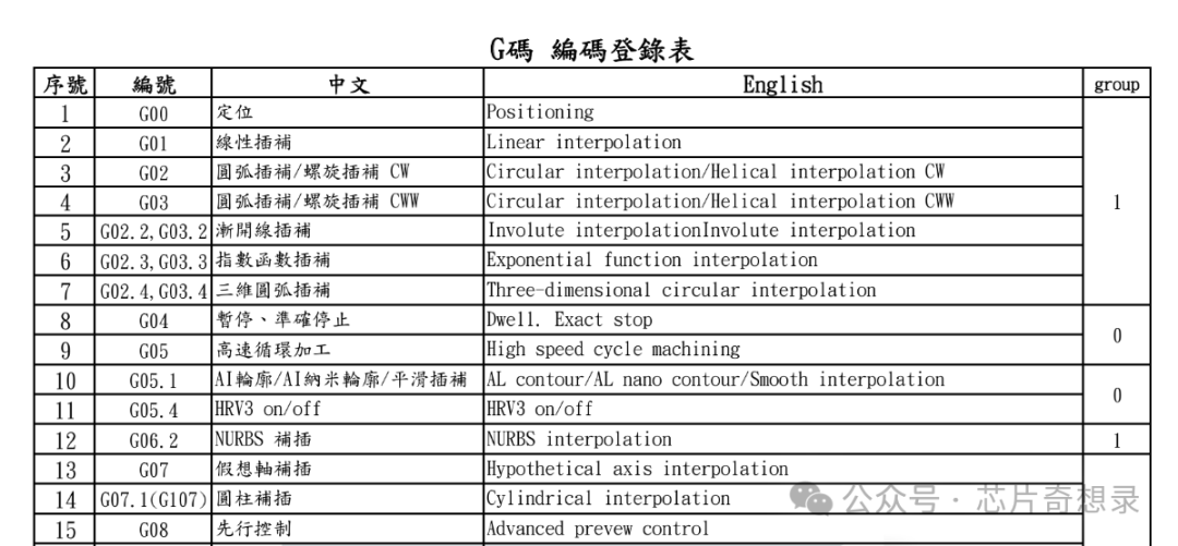
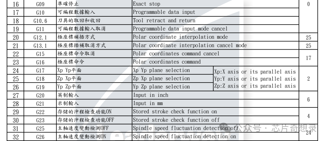
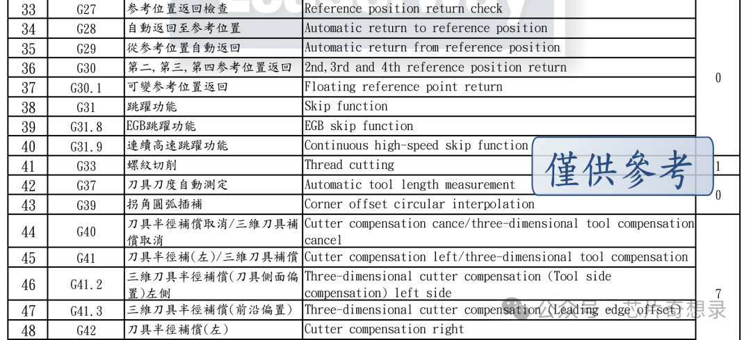
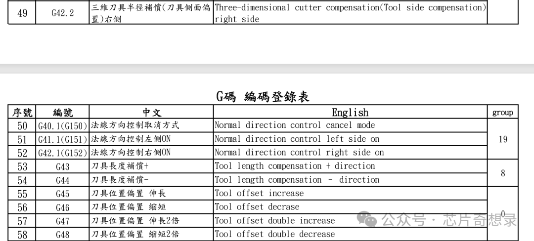
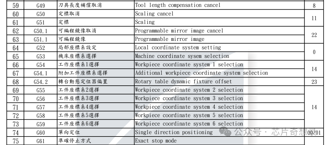
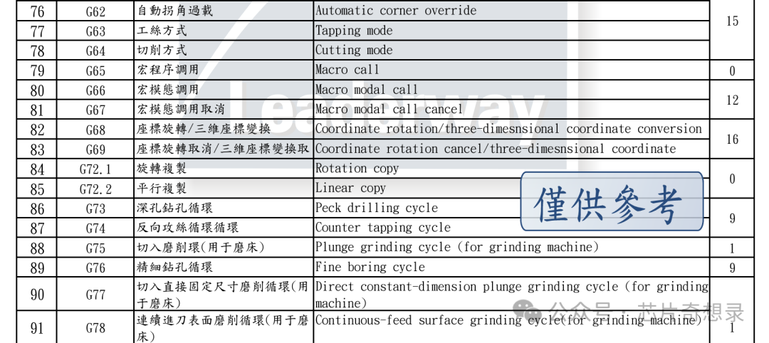
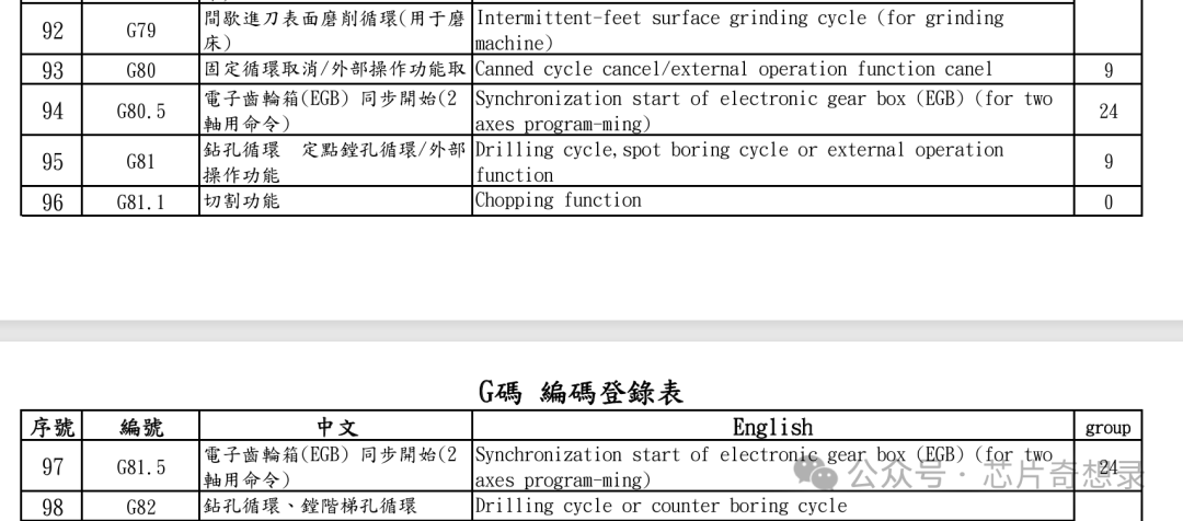
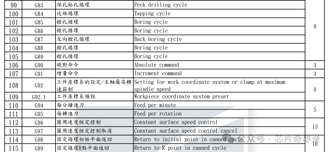
 * I remember the source document seems to have been downloaded from a company website in Taiwan, so this file is definitely incomplete, for example, the M parts (M00, M03, etc.) are missing. If I have time, I will look for them.Reference links:https://www.cnblogs.com/yangyang13/p/18776713
https://blog.csdn.net/AMDDMA/article/details/100176753
https://prodocs.lceda.cn/cn/pcb/export-pcb-fabrication-file-gerber/index.html