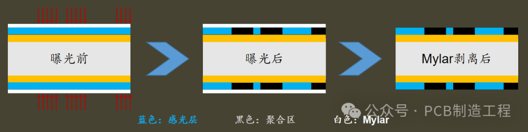
After exposure, the PCB board needs to have the Mylar on the dry film stripped before entering the DES process. Of course, PCBs using wet film technology do not have the issue of Mylar and do not require its protection.
Stripping Mylar
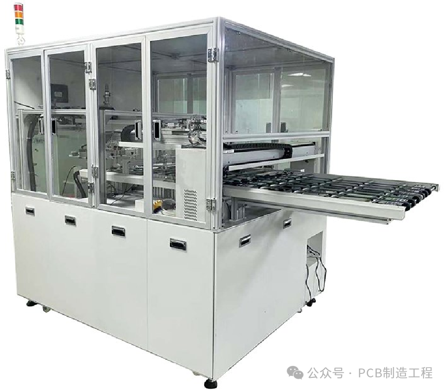
Mylar stripping can be done manually or using automated equipment.
Example of Mylar stripping equipment (Image source from the internet)
DES (Copper Reduction Method)
In PCB manufacturing, the traditional DES process is an integrated production line device that includes developing, etching, and stripping functions.
The name DES comes from the initials of the three English words: Developing, Etching, and Stripping.
The purpose of DES is to remove the dry film/wet film that has not undergone polymerization reaction through developing, then etch away the exposed copper foil, and finally strip the dry film/wet film covering the copper surface to create the desired circuit pattern.
-
Developing: Using chemical methods to remove the unexposed dry film/wet film, exposing the copper foil areas that need to be etched.
-
Etching: Using chemical methods to etch away the copper foil exposed during the developing stage.
-
Stripping: Using chemical methods to remove the remaining dry film/wet film on the PCB board, revealing the desired pattern.

DES Process Flowchart

|
Name |
Function |
|
Board Loading |
The board loader transfers thePCBinto the DESline |
|
Developing |
Removes the unexposed dry film/wet film |
|
Washing |
Washes away the residual chemicals on the copper surface from the PCB process to avoid contamination in subsequent processes. |
|
Etching |
Etches away the copper foil exposed during the developing stage |
|
Stripping |
Removes the remaining dry film/wet film |
|
Acid Washing |
Neutralizes the stripping alkaline solution |
|
Drying |
Blows dry/dries the board surface to avoid water residue. |
|
Board Unloading |
Stores the board in a temporary rack |
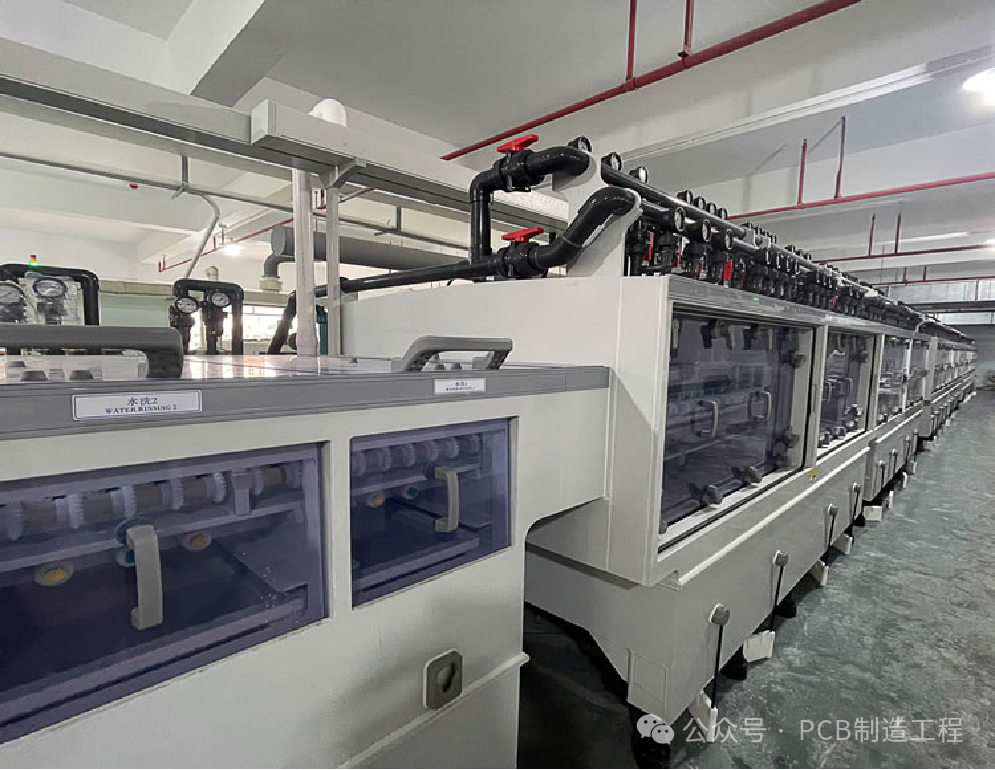
Example of DES line (Image source from the internet)
DES (Additive Method)
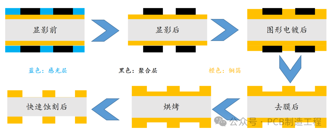
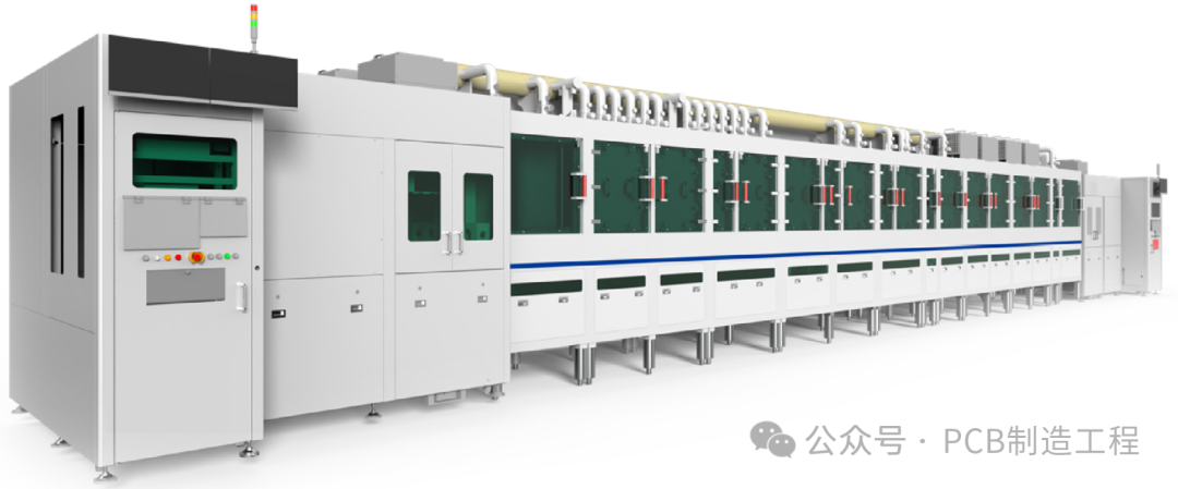
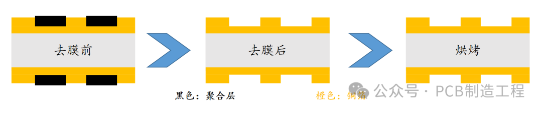
The additive method circuit process includes vertical developing (VDL), stripping, and fast etching lines.
-
Vertical Developing
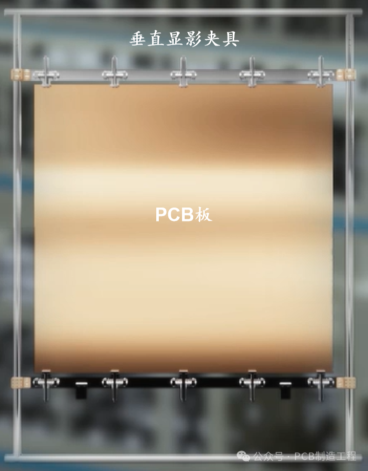
Vertical developing, as the name suggests, involves fixing the PCB board vertically through the fixture during the developing process. The reason for choosing the vertical method is that the rollers in horizontal developing lines can affect the quality of the dry film during transmission, and the additive method has high quality requirements for the dry film. If there are defects in the dry film that should remain on the PCB board during the developing process, it will increase quality issues during the plating process.
Example of vertical developing line (Image source from the internet)
Example of vertical developing PCB board fixture (Image source from the internet)
-
Stripping
-
Fast Etching
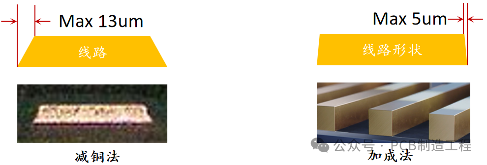
Fast etching, also known as Flash Etching, is a process in the additive method where the copper foil etched away includes base copper and chemical copper, while in the copper reduction method, the etched copper foil includes base copper, chemical copper, and electroplated copper.
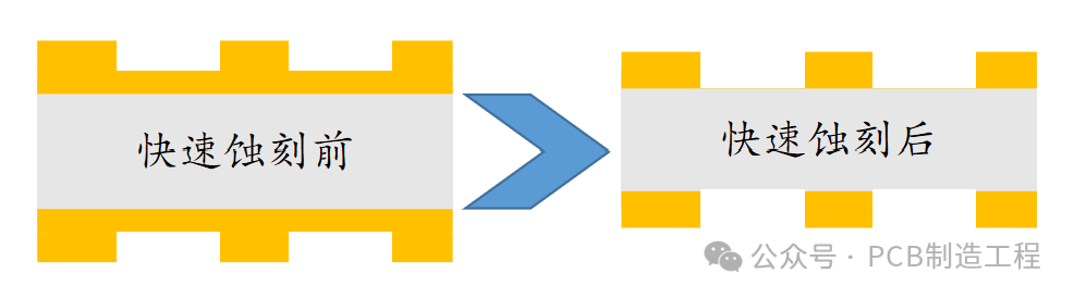
Examples of circuit morphology for copper reduction and additive methods
Important Concepts
-
Developing Point (Exposed Point)
Developing Point (%) = Distance from the copper exposure point to the start of the developing section / Total length of the developing section * 100.
Assuming the length of the developing section is 1.5M, when the copper board reaches 0.6M and starts to leak copper, that is: 0.6/1.5*100%=40%, then the developing point is 40%.
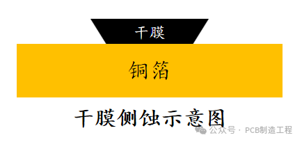
Typically, the developing point is controlled within 40%-60% of the total length of the developing section. If the developing point is too close to the exit of the developing section, the unexposed photosensitive layer will not be sufficiently developed, resulting in incomplete development; if the developing point is too close to the entrance of the developing section, the exposed photosensitive layer will have prolonged contact with the developing solution, causing edge film debris or undercutting of the dry film.
-
Etching Factor
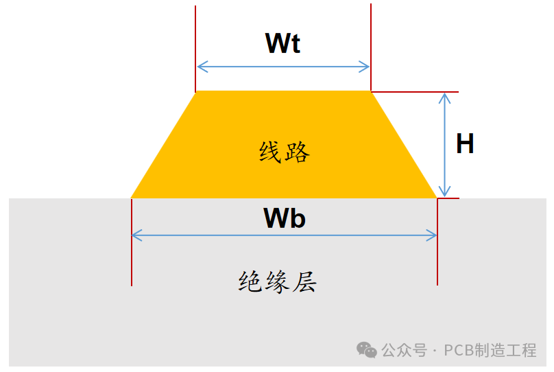
H: Copper foil thickness
Wt: Width of the line on the upper side
Wb: Width of the line on the lower side
Etching Factor F = 2H/(Wb-Wt)
The etching factor measures the difference in width between the upper and lower lines after etching.
The smaller the difference in width between the upper and lower lines, the better, meaning a larger etching factor indicates stronger etching capability of the PCB manufacturer.
Conclusion
Whether using the copper reduction method or the additive method, the goal of the line DES process is the same: to complete the production of the PCB circuit pattern.
In PCB manufacturing, the choice of process is closely related to customer requirements, graphic design, costs, etc. Typically, traditional PCBs and general HDI use the copper reduction method, while high-end PCBs, such as SLP and substrates, use the additive method.