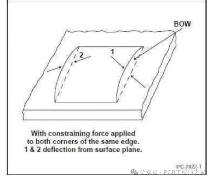
PCB warpage refers to the out-of-plane deformation of printed circuit boards that occurs after they are removed from the pressing fixture or specific environment, which does not meet design requirements. It can generally be subdivided into two forms: ✒︎ Bowing
Deformation resembling a bowl or arch bridge, where the four corners of the PCB are in the same plane, and the center is either bulging or depressed. This is the most common type.
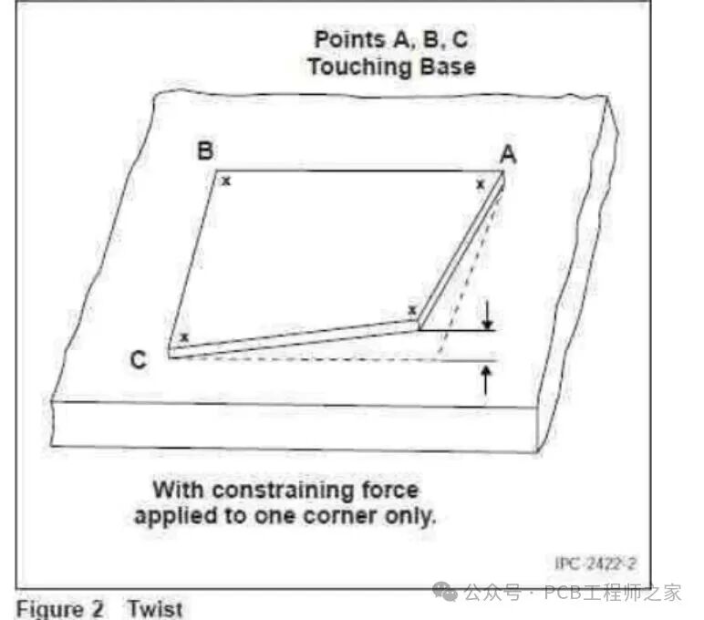
✒︎ Twisting
Deformation resembling a twisted shape, where three corners of the PCB are in one plane, and the other corner is raised. This is a more tricky and critical defect.
Warpage is not just “unsightly”; it can cause serious issues for subsequent assembly and product reliability. 1. Difficulty in Surface Mount Technology (SMT) On the SMT line, an uneven board can lead to inconsistent solder paste thickness, unstable component pickup by the nozzle, and components being suspended or standing upright after placement. 2. Poor Soldering Warped boards may exacerbate deformation during the reflow soldering process due to thermal expansion and contraction, leading to defects such as solder bridging, cold solder joints, and voids. 3. Difficulty in Through-Hole Component Insertion For boards with through-hole components, pins may not be able to smoothly insert into the holes. 4. Testing and Assembly Issues ✒︎ During in-circuit testing, probes may not make good contact with test points, leading to false readings. ✒︎ During final product assembly, the board may not be securely fixed within the casing, potentially causing stress. 5. Long-term Reliability Risks After forcibly correcting the installation of the board, internal stresses may persist, potentially leading to copper foil fractures and hole copper cracks, affecting product lifespan. The essence of warpage is the imbalance of stress across different layers or directions of the PCB. This stress mainly arises from materials and manufacturing processes. 1. Core Material – Copper Clad Laminate ✒︎ CTE Mismatch
This is the fundamental cause of warpage. PCBs are primarily composed of fiberglass cloth and resin, as well as copper foil. 𓀥 Fiberglass cloth (such as FR-4) has a low CTE in the X-Y direction, while resin has a high CTE in the Z-axis direction. 𓀥 The CTE of copper foil also differs from that of the core material. 𓀥 During lamination and cooling, different materials shrink at different rates, and if the design or process is improper, internal stresses can arise, leading to warpage.
✒︎ Material Properties 𓀥 TG Value: Low Tg materials have poor heat resistance and are more prone to softening and deformation at high temperatures. For lead-free soldering and other high-temperature processes, it is recommended to use high Tg materials. 𓀥 Material Symmetry: Asymmetrical stacking structures in multilayer boards are a primary design cause of warpage. 2. Design Factors ✒︎ Asymmetrical Stacking Structure, for example:
𓀥 Asymmetrical copper foil thickness distribution (e.g., in an 8-layer board, L1/L2/L7/L8 use 1OZ, while inner layers L3-L6 use 0.5OZ).
✒︎ Improper selection of core board and prepreg type and thickness, leading to uneven stress in the Z-axis direction. ✒︎ The core board is not symmetrically centered in the Z-axis direction. ✒︎ Uneven distribution of traces: One side of the board has a significantly larger copper area than the other. For example, the top layer has a large area of copper, while the bottom layer only has sparse signal traces. After etching, a large amount of copper is removed, resulting in a significant difference in shrinkage forces on both sides, causing the board to bend towards the side with more copper. 3. Manufacturing Process ✒︎ Lamination Process 𓀥 Rapid heating/cooling rates may not adequately release internal stresses. 𓀥 Uneven temperature of the press heating plate. ✒︎ Solder Mask and Character Printing The curing of solder mask ink itself can generate shrinkage stress. If the thickness or curing degree of the solder mask layer on both sides of the board differs, it can introduce new warpage. ✒︎ Thermal Treatment Processes Such as hot air leveling and reflow soldering, improper cooling after exposure to high temperatures can lead to warpage. ✒︎ Storage and Handling Storing the board vertically or in a humid environment can also lead to deformation.
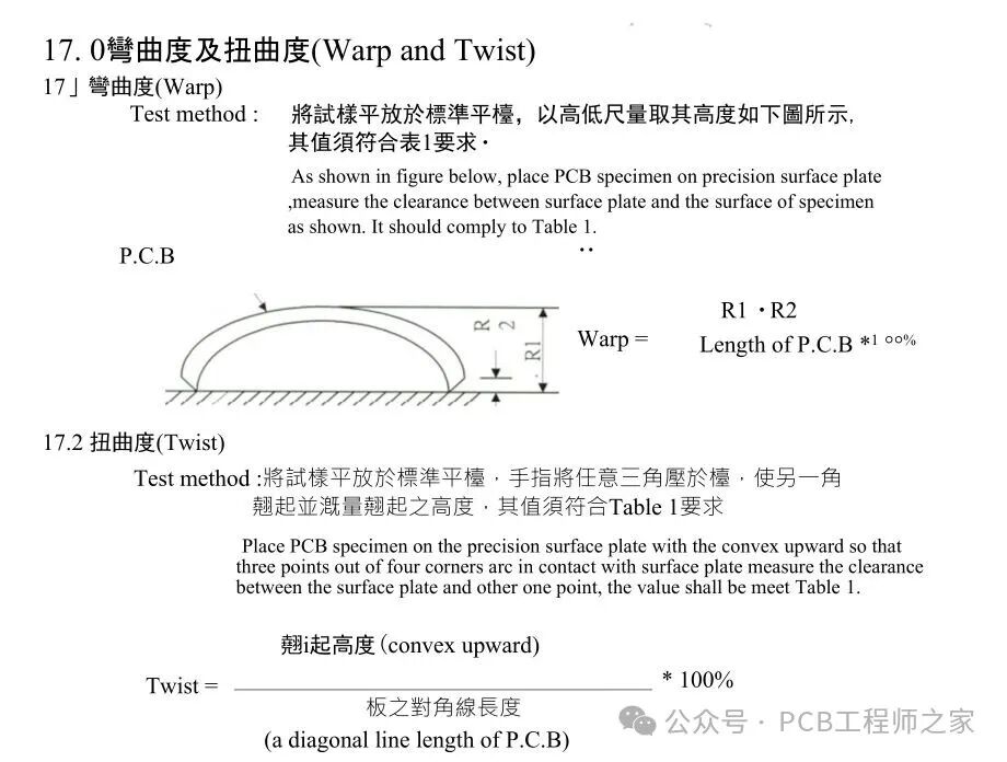
Measuring and Evaluating Warpage Industry standards typically use the IPC-TM-650 2.4.22 method. ✒︎ Formula
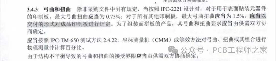
Warpage = (Maximum Deformation Height / Diagonal Length of the Board) × 100% ✒︎ Standard requirements are shown in the figure below:
 ✒︎ Measuring Tools: Dedicated warpage testing instruments, or simply placing the board flat on a marble platform and measuring the maximum gap with a pin gauge.
How to Prevent and Improve PCB Warpage?1. Design Phase ✒︎ Symmetrical Stacking Design
Ensure that the core board, prepreg, and copper thickness are symmetrically distributed around the Z-axis centerline.
✒︎ Balance Copper Area
Add balancing copper in layers with less copper. This is not for electrical grounding but to add non-functional copper to balance stress. ✒︎ Choose High-Quality Materials
Select high Tg, low-CTE, or high-reliability copper clad laminates based on product applications. 2. Manufacturing Phase ✒︎ Optimize Lamination Process: Use reasonable heating/cooling curves to allow resin to flow adequately and cure slowly, releasing stress. ✒︎ Bake Boards: Bake the boards before critical processes (such as LDI and solder mask) to release internal stress. ✒︎ Use Fixtures: Use fixtures or trays during processes like reflow soldering to limit board deformation at high temperatures. ✒︎ Cooling and Shaping: After exiting the laminator, use a cooling press or specific cooling racks to ensure the board cools evenly under pressure. PCB warpage is a complex, multifaceted issue involving materials, design, and processes. Solving it requires systematic thinking, starting from symmetrical design and implementing meticulous process control throughout the manufacturing chain. For engineers on the PCB manufacturing side, understanding and mastering warpage knowledge is one of the key skills to ensure high product quality and high yield rates.
This public account will continue to update information related to PCB/FPC design and manufacturing, please “follow“ to avoid missing the content you need…
If this has been helpful to you, please bookmark➕share➕like, thank you!
Previous Exciting Content:
Segmented Gold Finger Production Process and Control
PCB Impedance Matching and Software Calculation
Current/Resistance/Capacitance/Inductance Calculation
Rigid-Flex PCB Issues and Solutions
Analysis of PCB Manufacturing Defects and Causes
Common PCB Design DFM Traps
Basic Knowledge of PCB Materials (2)
Basic Knowledge of HDI (1)
Analysis of PCB Manufacturing Defects and Causes
Basic Knowledge of Back Drilling
Interpretation of IPC-4103 High-Speed and High-Frequency Materials
At everyone’s request, a PCB technology exchange group has been established; feel free to join if needed…