Follow our official account: Original Design Sharing by Attack City.【All articles are completely free, available for viewing anytime after following】】A treasure trove of development materials for embedded engineers, providing chip information and design references.//==================================================//
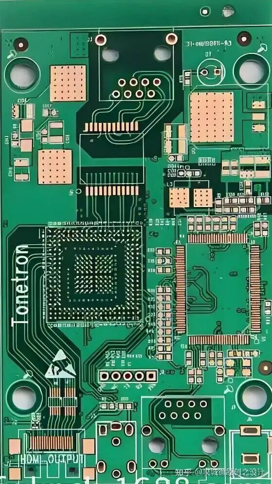
PCB, short for Printed Circuit Board, is a crucial component in electronic products. It is responsible for energy conversion related to circuits and supports the control and implementation of various functions by software. The PCB itself is made up of substrates and various metal connections, typically manufactured by specialized producers, as shown in the image below:
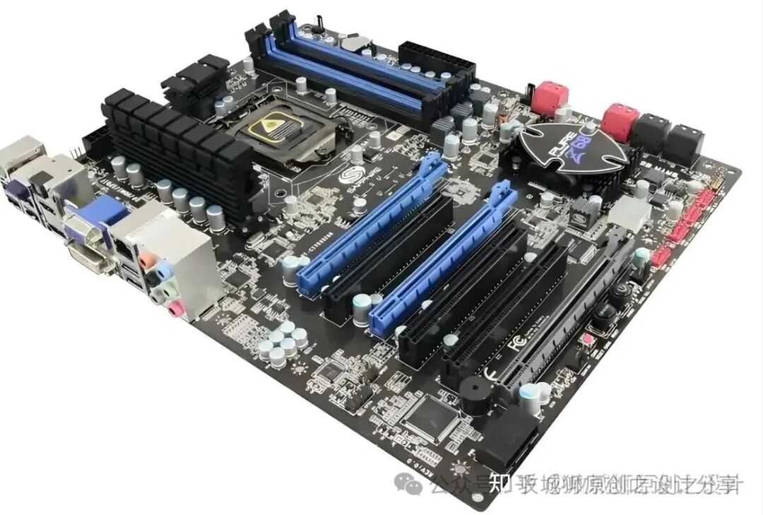
All electronic materials are soldered onto the circuit board, integrated with the lines on the board, forming the complete hardware of the controller. After injecting the software program and placing it in the product casing, it becomes a finished product. The physical image is as follows:
PCB design, in product design, is generally handled by hardware engineers or, in larger companies, by specialized layout engineers. The main task is to convert the schematic design into a physical circuit board design and output the design files for processing.
PCB design requires extensive knowledge. First, one must be able to understand schematic design. If the same person is responsible for both the schematic and PCB design, understanding the schematic is not difficult. If the roles are separated, the designer must fully comprehend the schematic and requirements set by the hardware engineer. Typically, both parties agree on the design, and finally, they confirm whether the completed PCB meets the schematic requirements, including component placement, height requirements, structural requirements, testing requirements, signal quality requirements, etc.
PCB design engineers also need to collaborate with structural engineers, as the casing limits the PCB’s dimensions, shape, and height constraints for components, ensuring correct assembly and compliance with thermal performance requirements.
When designing, PCB design engineers must pay attention to important circuit layout choices, high current path routing design, high-speed signal processing, circuits that generate radiation, circuits susceptible to interference, and overall board EMC performance optimization, among many other details. They must also consider material selection, PCB processing technology, component heat dissipation, electrostatic protection, and various design points. Completing a PCB design requires significant thought and consideration, especially for digital circuits that use more than six layers, high-speed signal optimization, high-power analog circuit boards, and RF signals, all of which impose high requirements on PCB design.
In some companies, PCB design engineers are also responsible for part of the simulation work, including signal quality simulation, power integrity, signal integrity, crosstalk, signal overshoot, ringing analysis, and optimization. The more complex the PCB, the more experienced and skilled the engineer must be to complete the design.

PCB engineers play a vital role in the design process from circuit schematics to PCBA production. The more complex the product, the more critical the PCB design becomes.
Today’s sharing ends here. We welcome everyone to like, follow, and share. If you have any content to add or thoughts, please leave a comment in the section below.Selected previous articles:In-depth analysis of the reasons for involution among workers and its harm to societyHow can beginners grow into hardware engineers?