1. Power Connector Design Standards
-
Electrical Clearance and Creepage Distance
-
The electrical clearance between the power and protective ground (PGND) should be ≥2mm, and the creepage distance should be ≥2mm (before the fuse) or ≥1.4mm (after the fuse).
-
The distance between PGND and other signals (such as GND, low-speed signals) should be ≥2mm, and the interface isolation distance should be ≥100mil.
-
High Voltage Area (-48V System):
-
General Connectors: Must verify pin spacing according to voltage level; dedicated power connectors (e.g., ATCA Zone 1) may be exempt.
-
Inspection Method: Highlight the network using PCB tools and manually measure the spacing in critical areas.
Current Carrying Capacity
-
Connector selection must meet the maximum load current (including abnormal short-circuit current), ensuring that the PCB copper foil burns out before the connector.
-
General connectors should optimize the distribution of power/ground pins to reduce current path impedance.
-
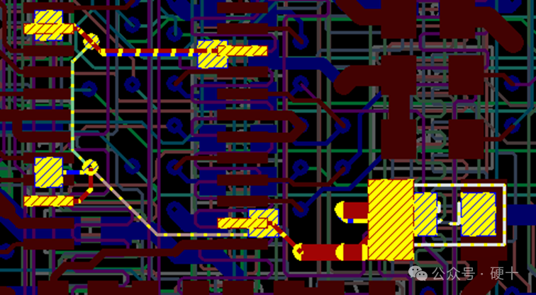
Diodes/Inductors/Magnetic Beads: The width of the traces before and after should be consistent to avoid sudden changes; the trace width on both sides of the RC filter resistor should match.
As shown in the figure below, after isolating the magnetic bead, it supplies power to the4 power pins of the device, but the trace is too thin, with a width of only5mil;
2. Power Layer and Copper Pour Design Standards
-
Copper Pour Current Carrying Capacity
-
Calculate trace width using formulas or tools (experience value: 1Oz thickness PCB, 40mil carries 1.5A), covering both normal and abnormal currents (based on fuse melting current).
Example:
For-48V power, our primary concern is the current carrying capacity of the copper pour (-48V usually requires soft start and filtering before use, so the power layer will not be laid out) and creepage distance. The copper pour should consider whether the current carrying capacity is sufficient, which must account for both normal and abnormal conditions, meaning if the board shorts, it should ensure that thePCB does not burn out first. If the device burns out, replacing it isOK, but if thePCB burns out, the entire board is scrapped, so it must first ensure that thePCB does not burn out. How much current should the copper pour’s current carrying capacity meet? This depends on the specific application, and a trick is to use the-48V fuse current as a standard; as long as the copper pour’s current carrying capacity is greater than the maximum current of the fuse, it can ensure that thePCB does not burn out. Experience data indicates that every40mil can carry
1.5A of current.-48V power copper pour’s current carrying capacity needs to be reviewed along the power supply path until-48V enters the power plane.For example, in the figure below, two-48V paths go from the connector through the copper pour to two fuses, with the maximum current of the fuse being
5A , and the width of the copper pour is about120mil, resulting in a current carrying capacity of only 4.5A , which is less than the fuse melting current of 5A , so thePCB may burn out first. 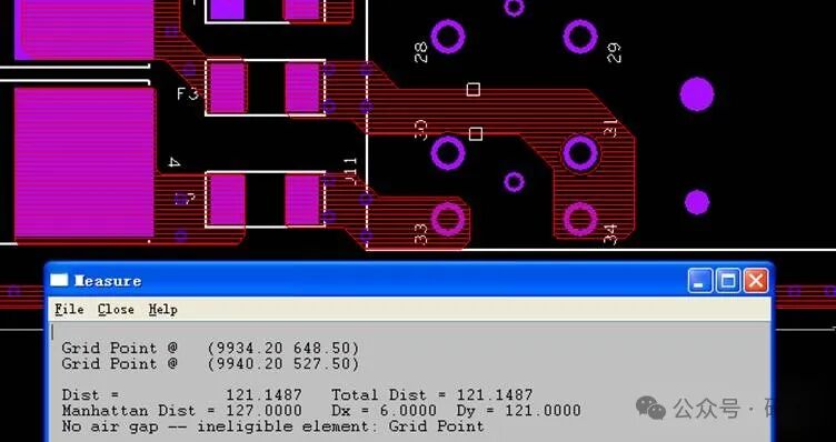
-
High Voltage Area (e.g., -48V): Prioritize solid copper pour, avoiding narrow bottlenecks; the entire path’s current carrying capacity must be ≥ fuse capacity.
Plane Layer Design
-
Power Layer Inset: The power plane should inset ≥50mil relative to the ground plane and ≥20mil from the board edge.
-
Separation Line Width: Regular area ≥30mil, safety area ≥80mil, BGA area ≥20mil.
3. Via Design Standards
-
Via Current Carrying Capacity
-
Each via is designed for 1-1.5A (10mil hole diameter), and the total number of vias in the path should be ≥ maximum current / single via current carrying capacity.
-
Focus on secondary power modules (e.g., 12V→5V) and high current areas (e.g., FPGA power supply).
Via Layout
-
Vias should be evenly distributed when changing layers for power, avoiding concentrated bottlenecks; prioritize larger vias (e.g., 12mil/24mil).
-
High-speed signal vias should not pass through power-sensitive areas (e.g., under MOSFETs).
4. DC/DC Design Standards
-
Layout and Filtering
-
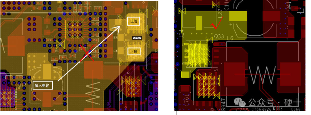
Input capacitors should be placed close to the upper MOSFET to shorten the high di/dt loop.
-
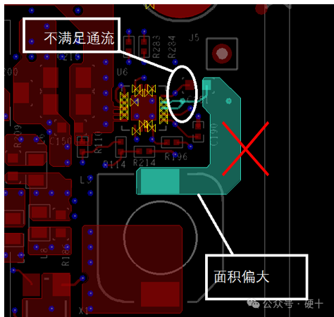
Reduce the area of the SW plane to minimize the copper area of dv/dt.
Feedback and Sampling
-
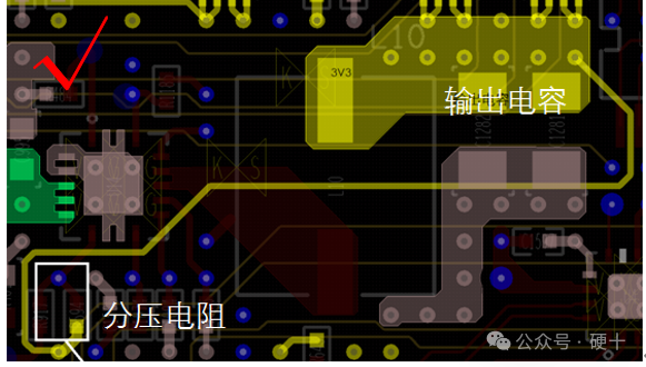
Voltage Feedback: High current power supplies use remote differential feedback, while low current uses local single-ended feedback; voltage divider resistors should be close to the controller.
-
Current Sampling: Differential routing, away from interference sources; sampling lines should be symmetrically drawn from both ends of the inductor.
Critical Routing
-
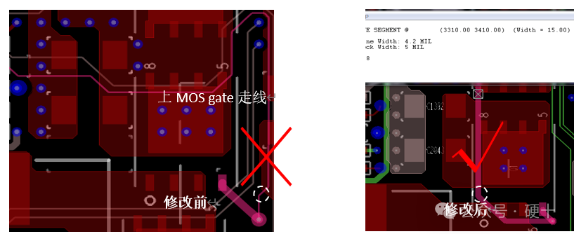
Drive Signals (GATE/BOOT): Trace width ≥15mil, minimize path length, avoid layer changes that create bottlenecks.
5. Sensitive Signals and EMC Protection
-
Signal Isolation
-
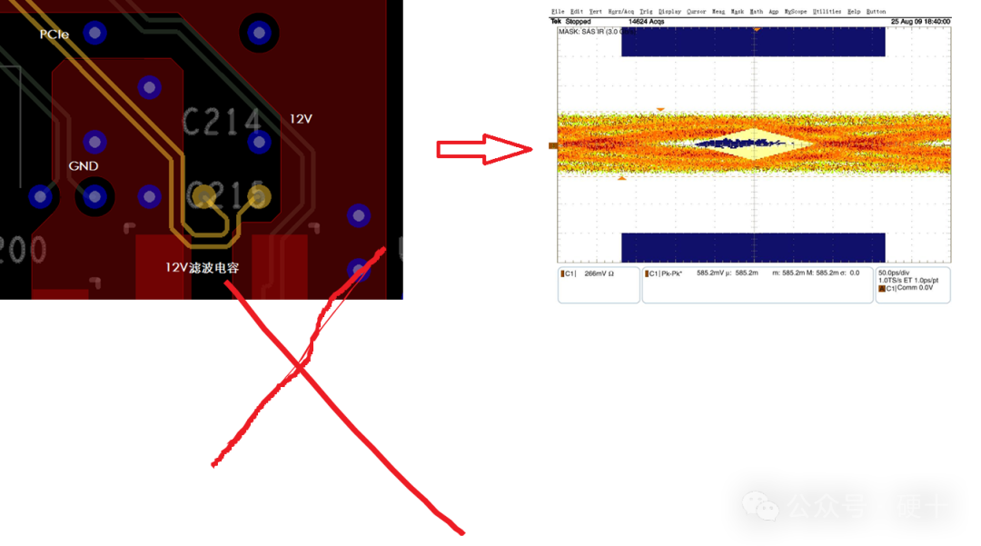
High-speed signals (e.g., PCIe, clock) should be kept away from the SW plane, with high-frequency current loops ≥100mil apart, avoiding parallel routing.
Ground Plane Optimization
-
Chip GND should be isolated from the power filter capacitor GND to avoid common ground noise coupling (e.g., LDO ground should be independently copper poured).
-
Sensitive circuits (e.g., PLL) should use local ground planes and be isolated by magnetic beads/inductors.
Noise Suppression
-
Large current DC-DC inputs should be connected in series with inductors (e.g., 1μH) and parallel filter capacitors (e.g., 470μF) to suppress switching noise coupling.
-
Heat dissipation copper should be treated with bright copper, and high-heat devices should be kept away from sensitive areas.
6. Thermal and Reliability Design
-
Thermal Design
-
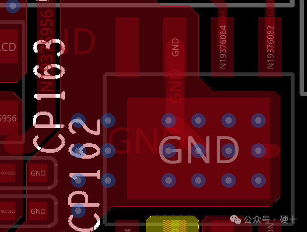
High-power devices (e.g., MOSFETs, power chips) should have large area copper poured underneath and added thermal vias.
Current Carrying Bottleneck Check
-
Focus on reviewing the effective width of power/ground in BGA, via dense areas, and narrow channels.
-
Simulate and verify voltage drop in high current paths (e.g., FPGA core power).
7. Safety Regulations and Process Requirements
-
High Voltage Area Handling
-
The distance between -48V and other low voltage power sources should be ≥2mm, and warning labels should be added in window areas.
-
Clear zoning before and after the fuse to avoid cross-zone wiring.
DFM Requirements
-
No crossing of input/output wiring for power modules to reduce return path interference.
-
Avoid right-angle routing for critical signal lines, preferring 45° or arc corners.
[Online Training] Intermediate Hardware Engineer (Single Board Power Design)