Introduction
Recently, I have been researching mechanical fault diagnosis and decided to create a small accelerometer, planning to use the STM32F1 as the main controller.
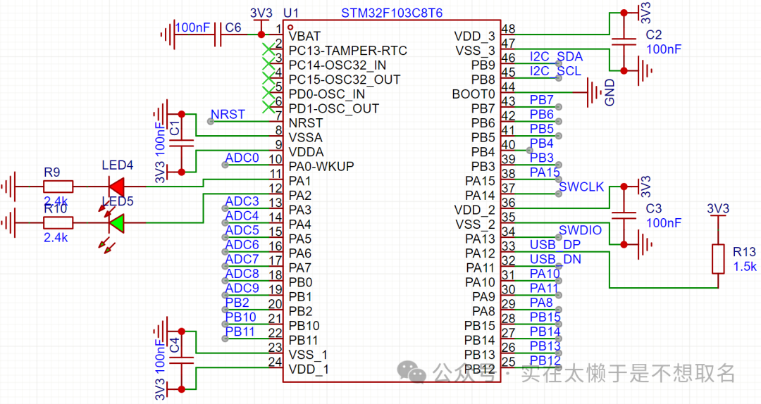
Initially, I planned to use an external crystal oscillator as the main clock for the STM32, but to further reduce the size of the board, I decided to remove the crystal and use the internal HSI as the main clock instead.
However, this design led to the USB not functioning at all. Indeed, it seems that the cleverness of a fool can sometimes surpass the convoluted thinking of a bad person.
In this article, we will take a look at the USB clock section described in the reference manual for the STM32.
1
STM32 USB Interface

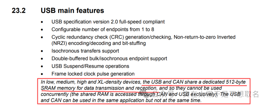
The STM32 USB interface connects USB 2.0 to the APB1 bus and emphasizes that the USB and CAN share a block of SRAM, so they cannot be used simultaneously.
USB and CAN can coexist, but they cannot be used at the same time.
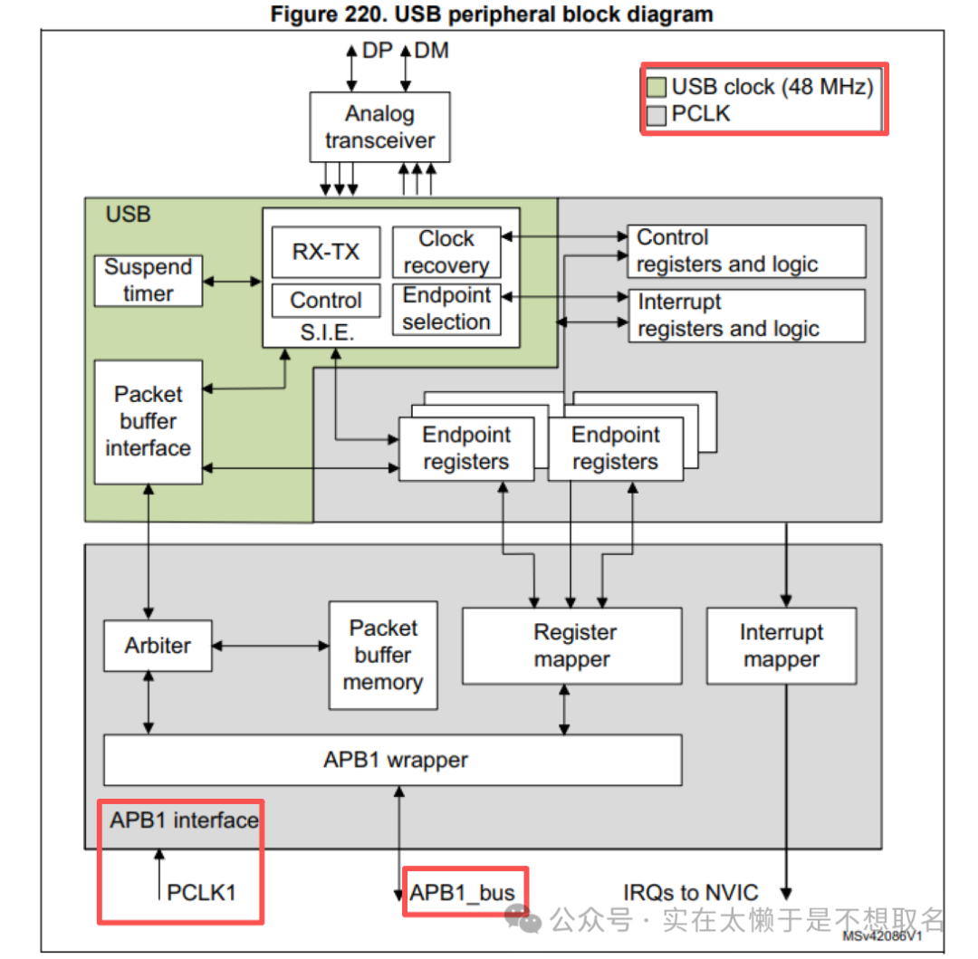
The main clock for the USB peripheral is provided by PCLK1, and it is essential to ensure that the USB clock is 48MHz. If the USB does not work for some users, it may be due to a mismatch in the clock design.
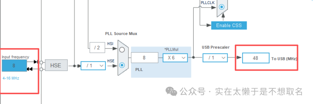
In STM32CubeMX, the default HSE clock is 8MHz, but if the user designs with a 12MHz crystal, although CubeMX shows the USB clock as 48MHz, the actual USB clock may be 64MHz, causing the USB to fail.
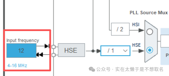
Therefore, it is necessary to modify the HSE clock to the actual clock to ensure the normal operation of the USB peripheral.
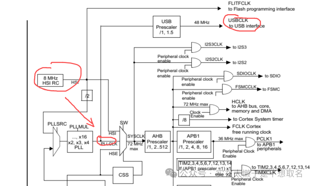
The USB clock comes from PLLCLK, and the manual also emphasizes that the HSI clock has a large error, so HSE should be used as the USB clock.
This is also the necessity of using HSE for the USB peripheral.
2
USB Workflow
The USB peripheral as a full-speed device interface begins its operation in the hardware initialization phase, first enabling the USB clock through the RCC register, configuring the USB control register to set basic device parameters, and establishing the endpoint buffer descriptor table to define endpoint types and double buffering mechanisms.
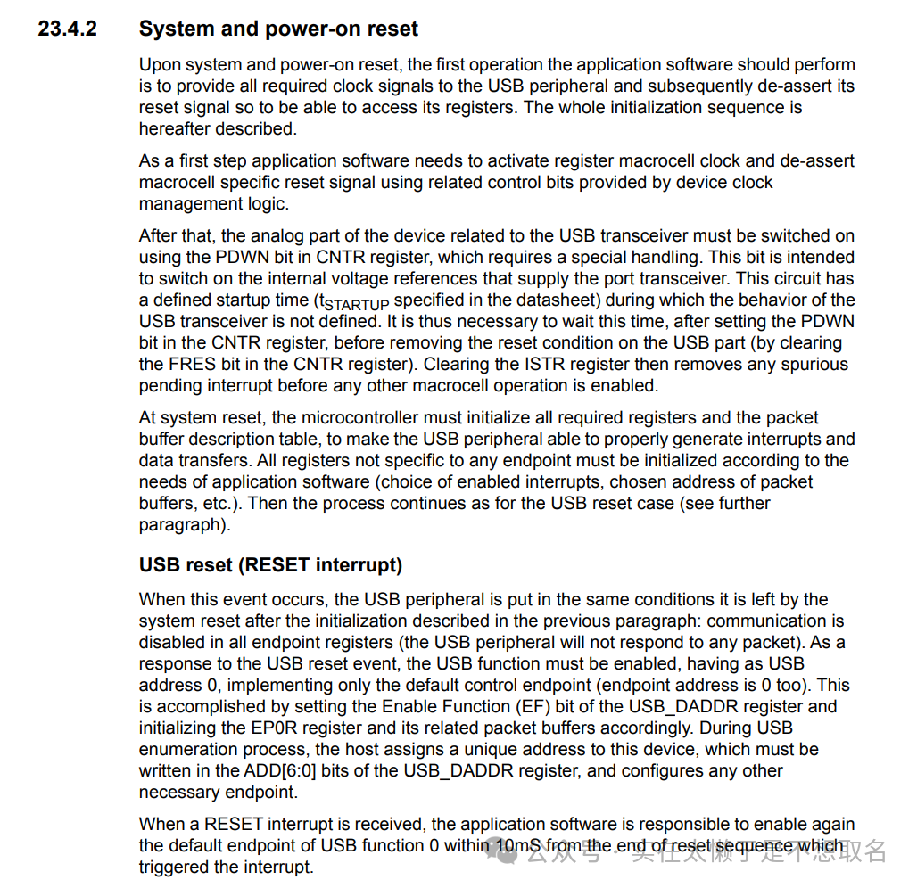
After powering on, the device automatically enters the default address 0 state, waiting for the host to initiate the enumeration process— the host requests the device descriptor through a control transfer, and the device firmware parses the SETUP flag of the USB_EP0R register, reads the pre-stored descriptor from Flash, and returns the data packet through endpoint 0’s IN transaction, completing address allocation and configuration switching (refer to section 23.4.1 of the documentation).
Once in the operational state, data transfer is interrupt-driven. When the host initiates IN/OUT transactions, the USB peripheral triggers a transfer complete interrupt, and the firmware reads the USB_ISTR register to identify the event source endpoint, then operates the corresponding USB_EPnR register: for bulk transfer endpoints, the double buffering mechanism allows filling the B buffer while transferring from the A buffer, achieving zero-latency switching by toggling the ADDTOG/STAT_TX bits; interrupt transfers utilize the NAK retry mechanism to ensure low latency, clearing the EP_KIND bit to send data when it is ready; isochronous transfers directly loop-write to the buffer without handshake packets.
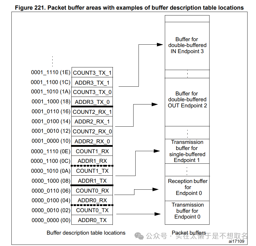
When receiving data, the firmware checks the CTR_RX bit of USB_EPnR, extracts data from the specified buffer address, and resets the buffer ownership. The error handling module monitors CRC errors or clock failures in real-time, triggering an automatic switch to HSI clock to restore communication.
If the bus is idle for more than 3ms, the USB peripheral automatically enters suspend mode, shutting down the main clock while retaining power for the 1.8V domain. At this point, the device can be woken up by external signals or remote wake-up— the firmware sets the RESUME bit of USB_CNTR to drive the bus K state, and the host restarts the clock upon detecting activity, allowing the device to rebuild the data link within 20ms. Throughout its lifecycle, descriptor management, buffer state machines, and interrupts work together to form an efficient pipeline, with the double buffering design significantly enhancing bulk transfer throughput.
The workflow concludes with the soft and hardware cooperative shutdown process: the firmware disables all endpoints, clears the PDWN bit of USB_CNTR to power down, and finally shuts off the clock.
3
Conclusion
This kind of error, which requires starting the entire design from scratch due to a single mistake, is not the first time. One should not rely on assumptions when designing circuits, and one should not easily give up when encountering problems.
Identifying the root cause of the problem and accumulating experience is indeed the path every electronic engineer must take.