When designing a PCB, I found that many people, especially beginners, do not have a clear understanding of the layers in a PCB. Therefore, today let’s take a look at the differences between the various layers when using the software Altium Designer to create a board.
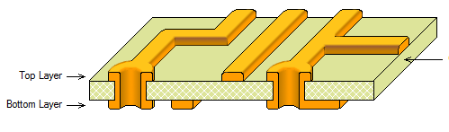
1. Signal Layer
2. Mechanical Layer
The Mechanical (mechanical layer) defines the appearance of the entire PCB. The emphasis on “mechanical” means that it does not have electrical properties, so it can be safely used to outline the shape, outline mechanical dimensions, place text, etc., without worrying about altering the electrical characteristics of the board. A maximum of 16 mechanical layers can be selected.
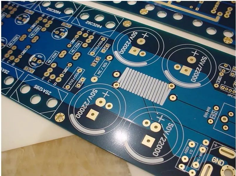
3. Silkscreen Layer
4. Paste Layer
5. Solder Mask Layer
The solder mask layer, often referred to as “window opening”, includes the top solder mask layer (Top Solder) and the bottom solder mask layer (Bottom Solder). Its function is the opposite of the paste layer, referring to the layer that is covered with green oil. This layer does not adhere solder, preventing excess solder from shorting adjacent solder points during soldering. The solder mask covers the copper traces to prevent rapid oxidation in the air, leaving openings at the solder points and not covering them.
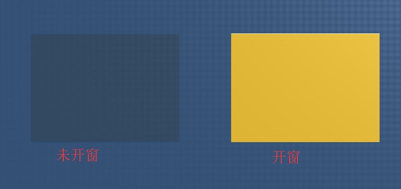
Regular copper cladding or routing is usually covered with green oil by default. If we process the corresponding area in the solder mask layer, it will prevent the green oil from covering and expose the copper.
6. Drill Layer
The drill layer includes Drill Grid (drill indicator diagram) and Drill Drawing (drill diagram) two drill layers, which provide drilling information during the PCB manufacturing process (such as pads and vias that require drilling).

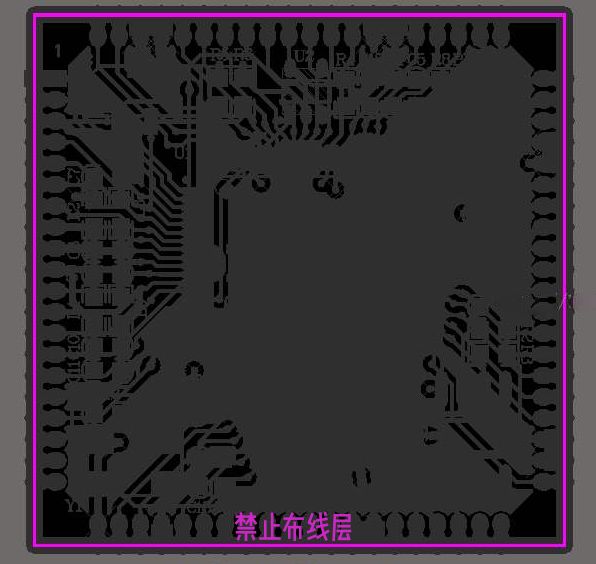
7. Keep Out Layer
The keep out layer (Keep Out Layer) is used to define the boundaries of routing layers. Once the keep out layer is defined, in future routing processes, the routing with electrical properties cannot exceed the boundaries of the keep out layer.
8. Multi-layer