PCB (Printed Circuit Board), also known as printed circuit board, is an important electronic component that serves as a support for electronic components and a carrier for electrical connections between them. It is called a “printed” circuit board because it is made using electronic printing techniques.
Its main function is to connect various electronic components through circuits, facilitating conduction and transmission; it is a key electronic interconnect component in electronic products. Almost every electronic device relies on printed circuit boards, as they provide mechanical support for the fixed assembly of various electronic components, facilitate wiring and electrical connections or electrical insulation, and deliver the required electrical characteristics. The quality of its manufacturing directly impacts the stability and lifespan of electronic products, as well as the overall competitiveness of system products, earning it the title of the “mother of electronic products”.
As an indispensable component of electronic terminal devices, the development level of the printed circuit board industry reflects, to a certain extent, the speed and technological level of the electronic information industry in a country or region.
Classification of PCB Products
PCB products can be classified in various ways, with the commonly used classification methods in the industry based on the number of conductive layers, product structure, and area.
Classification of Electronic Resins for PCB
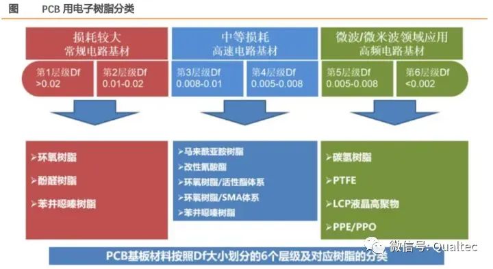
Electronic resins have different properties, each with its own advantages and disadvantages. Downstream customers often use various materials to complement each other’s strengths to achieve optimal overall performance based on different product applications.
Hydrocarbon Resins: These refer to polyolefin homopolymers or copolymers, including styrene-butadiene copolymers, polybutadiene homopolymers, polystyrene homopolymers, styrene/divinylbenzene copolymers, and styrene-butadiene-divinylbenzene copolymers.
Polytetrafluoroethylene (PTFE): PTFE has excellent dielectric properties, chemical resistance, heat resistance, flame retardancy, and low dielectric constant and loss in high-frequency ranges. However, due to its high viscosity in a molten state, it is usually formed using methods such as molding and sintering.
LCP: Liquid Crystal Polymer (LCP) is a new type of high-performance special engineering plastic developed in the early 1980s, featuring outstanding high-frequency dielectric properties, dimensional stability, and heat resistance, making it an ideal substrate for 5G high-frequency and high-speed circuit boards.
Polyphenylene Ether: Also known as poly(phenylene oxide) or polyphenylene ether, this high-strength engineering plastic developed in the 1960s is abbreviated as PPO or PPE. It has good mechanical properties and excellent dielectric performance, such as dielectric constant (Dk) and dielectric loss (Df), making it the preferred resin material for high-frequency printed circuit board substrates. However, it has a high melting viscosity, making it difficult to process; it has poor solvent resistance, which can lead to poor adhesion or detachment of wires during the solvent cleaning process in printed circuit board production; and its melting point is close to the glass transition temperature (Tg), making it difficult to withstand soldering operations above 250°C during printed circuit board processing. Therefore, PPE must undergo thermosetting modifications to meet the requirements of printed circuit board applications.
PI: Also known as polyimide, it refers to a class of polymers containing cyclic imide groups in their molecular chains, abbreviated as PI. Polyimide films are the best performing film-type insulating materials in the world, appearing yellow and transparent, with a relative density of 1.39-1.45. They exhibit excellent high and low-temperature resistance, electrical insulation, adhesion, radiation resistance, and dielectric properties.
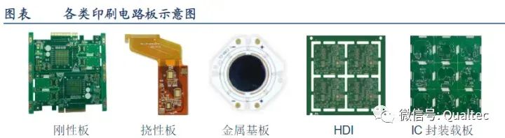
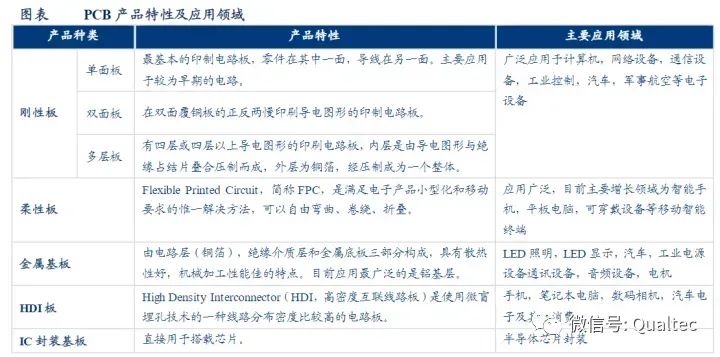
Classification by Structure
PCB products can be classified into single-sided boards, double-sided boards, flexible boards, HDI boards, and packaging substrates. Among the segmented product structures of PCBs, multi-layer boards have occupied a significant portion of the global PCB product structure, with a global market value of $21.1 billion for multi-layer PCBs in 2016, accounting for 39% of the global PCB market value; the global market value for flexible boards was $10.9 billion, accounting for 20% of the global PCB market value, with an increasing trend year by year; the global market value for single-sided boards was $8 billion, accounting for 15%; the global market value for HDI boards was $7.7 billion, accounting for 14%; and the global market value for packaging substrates was $6.6 billion, accounting for 12%.
HDI stands for High Density Interconnect, which refers to a type of printed circuit board that uses micro-blind/buried hole technology, characterized by a high circuit density. In the PCB industry, HDI boards are typically defined as having a minimum line width/spacing of 75/75μm or less, a minimum conductive hole diameter of 150μm or less, containing blind holes or buried holes, and a minimum pad size of 400μm or less, with a pad density greater than 20/cm2, classifying them as high-end PCBs.
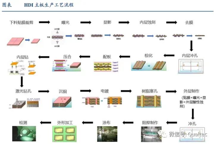
HDI mainboards are mainly divided into first-order, second-order, third-order, and AnyLayer HDI, with characteristic dimensions gradually decreasing and manufacturing difficulty gradually increasing. Currently, the most commonly used in electronic terminal products are third-order, fourth-order, or AnyLayer HDI mainboards. AnyLayer HDI, also known as arbitrary-layer or arbitrary-order HDI mainboards, is sometimes referred to as ELIC (Every Layer Interconnect) HDI. The most commonly used AnyLayer configurations in electronic terminal products are 10-layer or 12-layer. Apple introduced AnyLayer HDI for the first time in the iPhone 4S, and Huawei’s current flagship series mainly uses AnyLayer HDI, such as the Huawei P30 series mainboard, which is divided into Main PCB and RF PCB, both of which use AnyLayer HDI. The Mate 20 and Mate 30 series also use AnyLayer HDI mainboards.