In the previous article, we introduced methods forsystem-level low power design, such ashardware-software co-design,power management mechanisms, etc. This issue will delve into the core technologies ofarchitecture-level low power design, includingmulti-voltage design (Multi-VDD),dynamic voltage frequency scaling (DVFS),system clock optimization,asynchronous design, andalgorithm optimization. By reasonably dividing power supply areas, dynamically adjusting voltage and frequency, and optimizing clock architecture, power consumption can be significantly reduced while ensuring system performance.
1. Multi-Voltage Design (Multi-VDD)
The impact of voltage on power consumption is significant; therefore, multi-voltage design (Multi-VDD) is an important means of architecture-level low power optimization. The basic idea isto use different supply voltages based on the performance requirements of different modules, reducing power consumption while ensuring timing.
1.1 Multi-Voltage Techniques
Depending on the voltage management method, Multi-VDD mainly has the following three implementation methods:
(a) Fixed Voltage Division (as shown in Figure 1.1 (a)):
- Different modules are divided intofixed power supply voltage domains, and the voltage values of different voltage domains are constant;
- Suitable for chip designs with clear power and performance requirements, such as high-performance CPUs and low-power DSPs using different voltage domains.
(b) Predefined Multi-Voltage Modes (as shown in Figure 1.1 (b)):
- Each voltage domain can switch between multiple fixed voltages, withsoftware controlling the selection of the appropriate voltage mode;
- Suitable for systems that need to dynamically adjust power consumption based on load, such as CPU load regulation in mobile devices.
(c) Adaptive Voltage Scaling (as shown in Figure 1.1 (c)):
- The supply voltage of the voltage domain isvariable, which can be dynamically adjusted based on the operating state to achievemore precise power optimization;
- Suitable for high-end smart devices and data center servers, which can dynamically adjust voltage through intelligent power management algorithms.
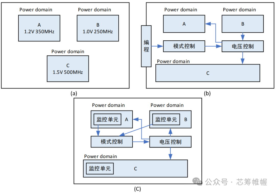 Figure 1.1 Three Methods of Multi_VDD
Application Case:Inmobile SoC design, the CPU may use different voltages, such ashigh-performance mode (1.2V),standard mode (1.0V), andlow power mode (0.8V), thus reducing power consumption while ensuring performance.
1.2 Power Gating
When a functional module is not needed for a period of time, its power can becompletely turned off to reduce dynamic power consumption. This technique is known as Power Gating. A schematic diagram of a structure with Power Gating:
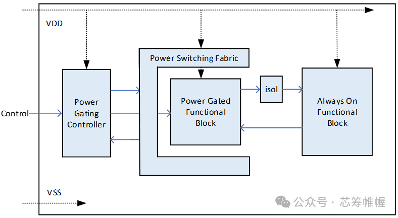
Key Points of Power Gating:(1) Completely turn off the power, which can completely eliminate dynamic power consumption;(2) May generate leakage power, as Power Gating requiresthe addition of Isolate Cell and Retention Cell, which can generate a small amount of leakage power themselves;(3) There is power overhead during shutdown/recovery, which involves the power charging/discharging process and requires fine management.
Due to the presence of capacitance, after the power is turned off, the voltage will slowly drop, leading to latch current (Crowbar Current) issues. Therefore, Isolate Cell is needed for protection (see 1.3).
1.3 Multi-Voltage Control Units
To ensure stable operation between different voltage domains, the following key units need to be added:
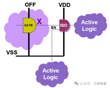
(1) Isolation Cell
- Prevents X-state from propagating to other voltage domains when one voltage domain is turned off.
- Mainly achieved byclamping the output signal of the shut-down domain to high or low levels to avoid interference.
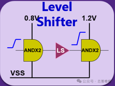
(2) Level Shifter
- Cross-voltage domain signal conversion, ensuring reliable data transmission between different voltage domains;
- Applicable for data, clock, scan chain, and other signals across voltage domain transmission scenarios.
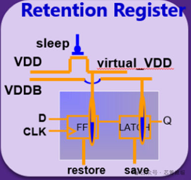
(3) Retention Register
- Retains key information during power-off, allowing for quick state recovery;
- Uses high Vt cells to reduce leakage power, but may affect timing.
1.4 Voltage Distribution
In multi-voltage design, how to reasonably divide the power supply area is crucial.
Generally, the delay of the unit is inversely related to the supply voltage, meaning that the higher the supply voltage, the smaller the delay.
(1) High-performance modules (such as CPUs, DSPs) use high voltage to reduce delay and meet high frequency operation requirements.(2) Low-speed peripherals (such as GPIO, UART) use low voltage to reduce power consumption.(3) Memory modules use moderate voltage to balance performance and power consumption.During design, it is necessary to comprehensively considertiming constraints, power budget, and design complexity to ensure that voltage division reduces power consumption without affecting performance.
2. Dynamic Voltage Frequency Scaling (DVFS)
DVFS (Dynamic Voltage and Frequency Scaling) is atechnology that dynamically adjusts voltage and frequency based on load, which can significantly reduce system power consumption.(1) Reduce voltage and frequency under low load to decrease power consumption;(2) Increase voltage and frequency under high load to ensure performance;(3) Hardware-software collaborative management to adjust clock and power supply strategies in real-time.
Application Case:The CPU in smartphones uses the DVFS mechanism to lower the main frequency during standby and increase the main frequency when running large applications to optimize power consumption and performance.
3. System Clock Optimization
The system clock isone of the main sources of power consumption, and reasonable clock management can significantly reduce power consumption.(1) Clock Gating, turning off unnecessary clocks to reduce toggling power;(2) Work Mode Management, such as Normal, Slow, Idle, and Sleep modes, dynamically adjusting clock frequency;(3) Local Clock Optimization, by partitioning clock domains to avoid unnecessary global clock switching.
| Mode | Description |
| Normal | Using PLL clock, sent to core and peripheral circuits |
| Slow | Using external clock |
| Idle | Only sending clock to peripheral circuits, turning off core clock |
| Sleep | Only providing clock to wake-up circuits, etc. |
4. Asynchronous Design
In some cases,asynchronous design is more energy-efficient than synchronous design. For example, in amulti-module system,each subsystem can use independent clocks instead of a unified global clock, thus reducing power overhead caused by global synchronization.
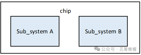 Figure 4.1 Synchronous Design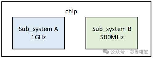
Figure 4.2 Asynchronous Design
5. Algorithm Optimization
In addition to hardware architecture optimization,algorithm optimization is also an important means of reducing power consumption. For example:
(1) Reduce multiplication operations and use addition instead to lower computing power consumption;(2) Reduce division operations and use shift operations to improve energy efficiency.For example, in NPU,using fixed-point operations instead of floating-point operations can significantly reduce power consumption.
6. Conclusion
(1) Multi-voltage design (Multi-VDD) —— Fine division of power supply domains to reduce overall power consumption;(2) Dynamic voltage frequency scaling (DVFS) —— Hardware-software collaboration to adjust power consumption in real-time;(3) Clock optimization —— Turn off unnecessary clocks to reduce dynamic power consumption;(4) Asynchronous design —— Avoid global clock synchronization to reduce power waste;(5) Algorithm optimization —— Choose more efficient computing methods to reduce computation power consumption.