To better serve everyone, I would like to report on the main business currently handled by me. For design outsourcing, friends with backend outsourcing needs are welcome to contact me (WeChat ID: ic-backend2018), and of course, if you have resources, you can also introduce them to me, and there will definitely be generous cash rewards (15% commission).
PS: The 27th IC backend training camp will officially start next week (4999 yuan training camp)! If you need to sign up, you can directly contact me.
The Low Power Quad-Core A7 Top Hierarchical Flow Physical Full Process Implementation Training Camp will also officially start in March!
Our main business in the IC community
1 Technical consulting (including technical problem consulting, project tapeout review, etc.)
Support for technical support for personal and company projects. Public-to-public transactions and invoicing are also supported!
2 Project outsourcing services (ranging from synthesis to GDSII out)
I have 12 years of experience in digital IC backend implementation, proficient in digital top, high-performance CPU, and complex clock structure design. Successfully tapeout over 40 large SOC chips, with the largest area being 150mm2.
The main processes involved include T55, T40, T28, T22, T16, T12, T7,S14, S8, GF40, GF28, GF22, SMIC55, SMIC40, SMIC28, SMIC14, SMIC12, UMC28, etc.
Support backend project outsourcing + targeted training for enterprise employees based on outsourced projects! Annual service for small companies starts from 80,000 yuan (one-time contracting of backend projects for the whole year)!
3 IC backend training camp
Provide high-end servers and actual company projects for students to practice (TSMC 28nm Cortex A7 core project), answering all students’ questions in a timely manner every day. If problems arise during practice, remote assistance can be requested to log in to the server to solve actual project issues.
Essential practical projects for IC fall recruitment (including all timing calculation question types)
For fresh graduates or those looking to change careers, this training camp can help you learn practical skills, and in about a month, you can get your ideal offer.
After the accumulation of the previous 26 training camps, the influence of our community training camp in the industry is growing, and its reputation is improving. Companies generally favor students from community training camps. It is no exaggeration to say that as long as students write our project on their resumes, they are basically prioritized for admission. The underlying logic behind this, everyone can ponder.
The overall knowledge system of the community training camp can be viewed by copying the link below to your browser.
https://alidocs.dingtalk.com/i/p/QqWXw073xd4Z2m31/docs/QqWXwnN058prxz31
The IC backend training camp will be fully upgraded in the future, and projects will include TSMC Double Pattern 12nm A72 (Maia_cpu) project, and the price will increase significantly. Therefore, the current 4999 training camp course will only be open until the next session (reserved for some students who book in advance), and later it will fully adopt the upgraded course (new course, new price).
The most comprehensive digital IC backend design implementation training tutorial
2023 Jieli Technology Digital IC Backend Written Exam Questions (The 24th IC Backend Training Camp is now open!)
Notice for the 25th IC Training Camp of the IC Community (only 2 spots left)
4 Knowledge Planet High-End Technical Learning and Communication Community
The high-end technical communication community operated by me—Knowledge Planet has also been running for nearly 6 years, gathering over 2780 star friends (currently the largest high-end paid technical community in the IC industry).
As the number of community members increases, the content operation and management costs of the community also rise. To continuously provide everyone with more comprehensive, systematic, and down-to-earth high-quality content, the community has decided to adopt a tiered pricing strategy, increasing the ticket price by 20 yuan for every 100 new members. The current ticket price has officially been adjusted to 328 yuan.
5 Graduate Design Guidance (only for digital IC backend implementation direction, can provide advanced process libraries and project data)
Provide quad-core A7/A55/A72 top-level low-power design implementation data and guidance, with processes available as needed, such as TSMC 28 or TSMC 16 (can also support 7nm processes). Students can base their papers on this project, with technical and writing guidance provided.
Recently, community IC backend training camp students asked why power switch cells should be added between memory channels in low-power design implementations, among a series of questions. Indeed, these issues are often encountered in actual company projects, and when I first started, I was also quite confused about them. Today, I take some time to summarize the related issues, hoping to be of help to everyone.
Why add power switch cells to the memory channel?
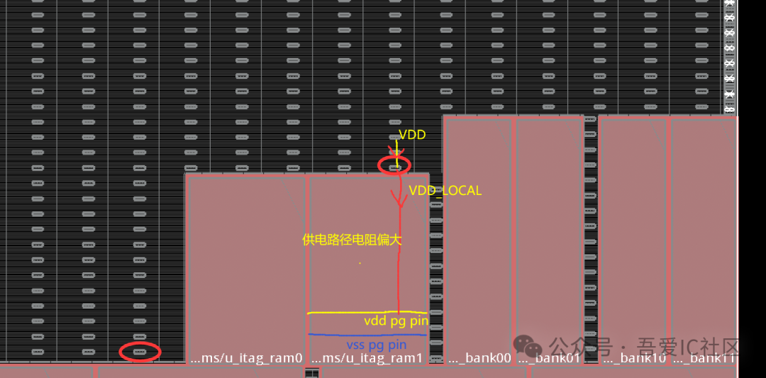
The memory we use in our project does not have power gating functionality. Therefore, its VDD pg pin (VSS is not turned off) should also be connected to VDD_LOCAL after the power switch cell.
After clarifying this point, let’s see why we need to add power switch cells. In the layout shown below, we assume that the memory channel does not have power switch cells, then the VDD pg pin on the memory must find power from the nearest Power switch cell. This way, the resistance of the physical power supply path from VDD_LOCAL to VDD PG Pin will be relatively large, resulting in a poor corresponding IR Drop.
Summary of methods to prevent IR Drop in the early stage of digital IC backend implementation
IR Drop analysis via Redhawk analysis process
The power switch cell essentially implements the power switch function from VDD to VDD_LOCAL. Therefore, adding power switch cells between memory channels provides more power switches near the memory.
Should power switch cells use common nwell type or two nwell type?
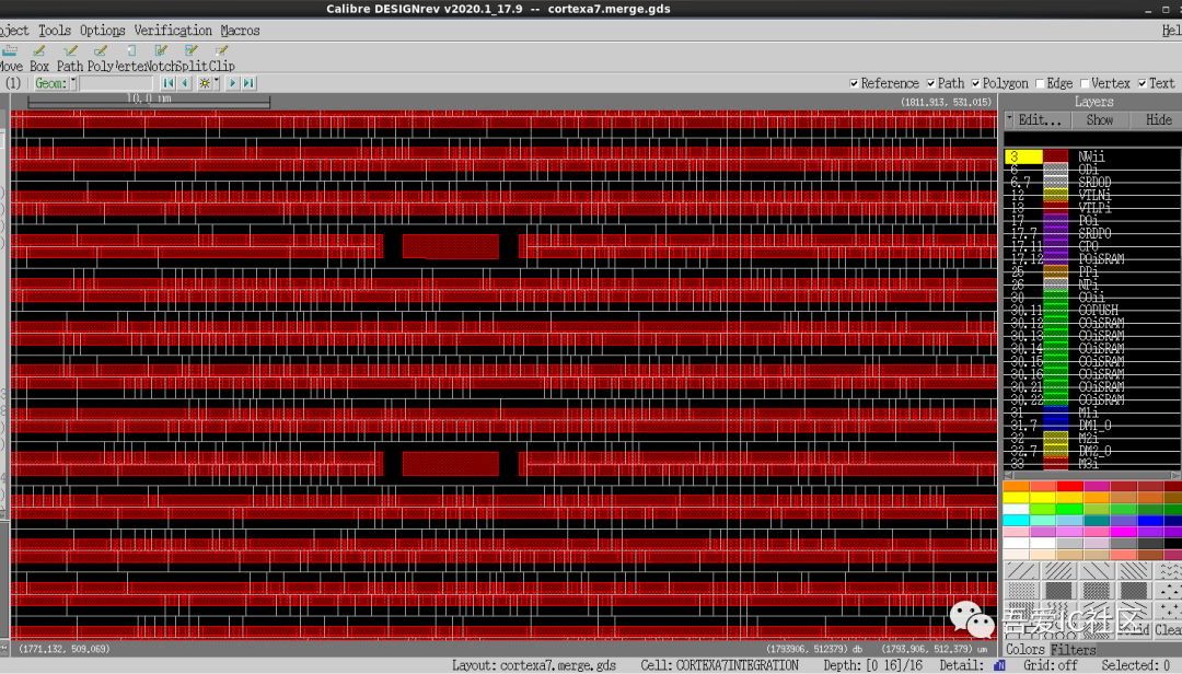
The diagram below shows the type of Power Switch Cell used in our low-power advanced training camp project. It is clear that its NWELL is separated from other standard cells.
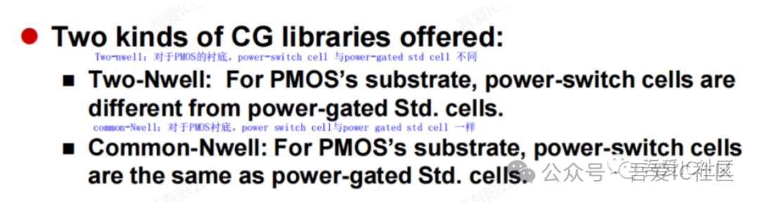
Of course, we can also use common nwell, but in this case, the nwell of the power switch cell and the nwell of the standard cells are completely adjacent, so this type of power switch cell must have an nwell biasing pin, and this pin needs to be connected to the global VDD net. This special nwell biasing pin needs to be routed according to the connection method of the secondary pg pin.
Summary of the connection method for secondary power pins in low-power design implementations
How should the size of the memory channel be reserved?
For channels that need to add power switch cells, the minimum spacing S=1*power switch cell width +2*endcap width +1*tapcell width.
In addition, the number of routing resources required by the memory itself must also be considered. Especially for the case where the pins of two memories face each other, it is necessary to evaluate whether enough routing resources can be provided within the channel range. If the minimum channel routing resources calculated above are insufficient, the size of the channel needs to be further increased.
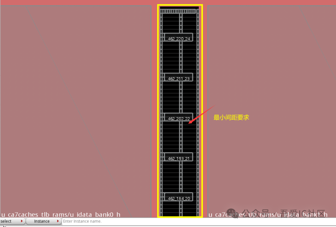
Of course, if the design does not have a power domain, then the spacing of this channel can be smaller, or even directly covered with hard blockage.
How to add power switch cells to the channel between memories?
For actual projects, we divide the addition of power switch cells into core areas and memory channel areas. When adding power switch cells to the core area, the channel must first be covered with hard blockage.
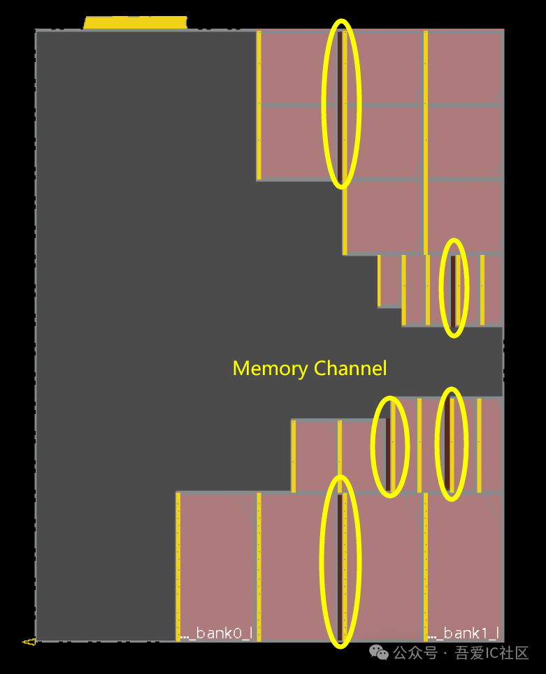
The effect of adding power switch cells to the core area using the command below is shown in the figure below.
[Thought Question] Why should power switch cells be added at the module boundary?
addPowerSwitch -column -powerDomain VDD_LOCAL -globalSwitchCellName HDRDID2BWP40P140 -leftoffset $mtcmos_core_offset -horizontalPitch 30 -noEnableChain -areaType boxlist -skipRows 4 -ignoreSoftBlockage -instancePrefix PSO_CORE_ -incremental -noFixedStdCellOverlap -bottomOffset 0.9br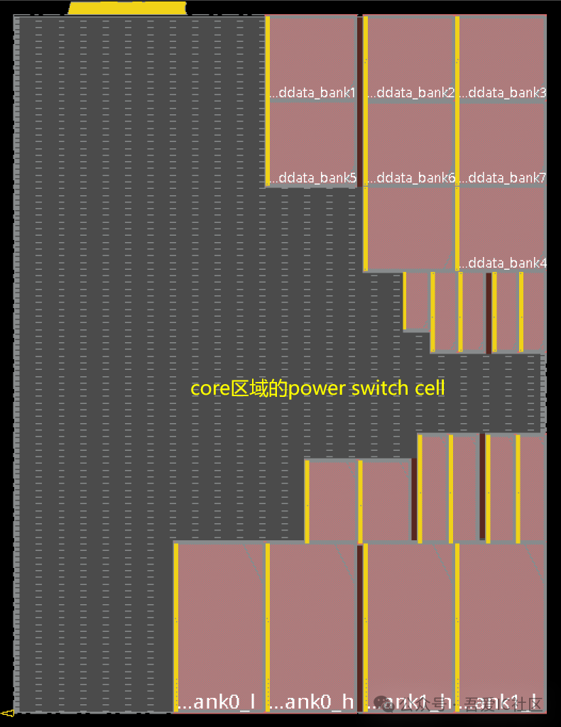
Using the command below to add PSO to the five channels in the design results in the following effect.
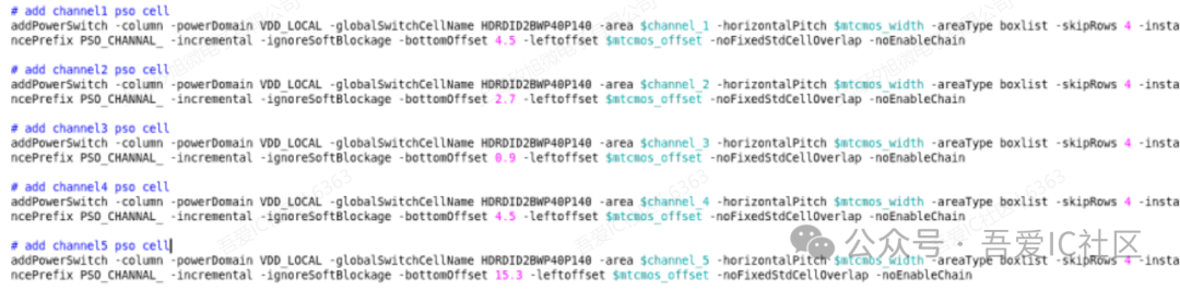
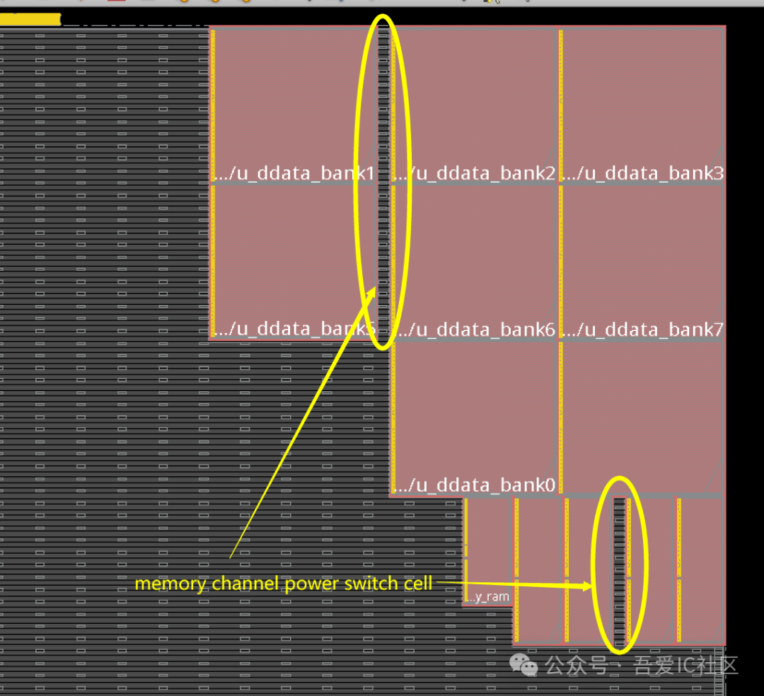
[Thought Question] What are the advantages and disadvantages of having too high a density of power switch cells in the memory channel?
After adding power switch cells to the channel, how to add power mesh to them?
Similar to adding PSO, before creating the power mesh network in the core area, the channel must be covered with routing blockage to avoid power stripes falling into the channel, which would affect the subsequent construction of the power supply network in the channel.
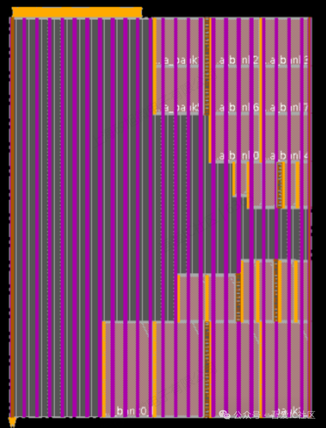
After adding routing blockage, first add the M9 power stripe to the core area outside the channel. It is necessary to cover each PSO with an M9 power stripe to strengthen the power supply.
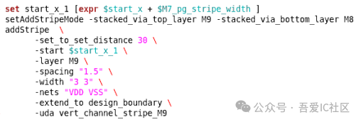
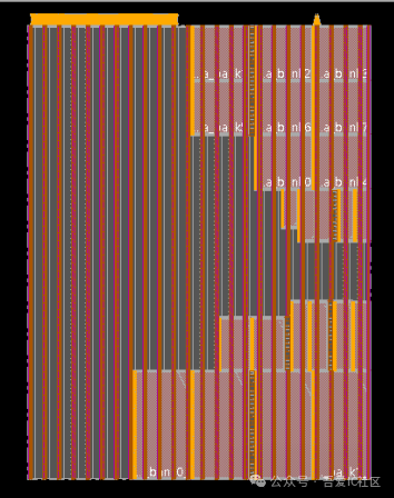
Next, we need to add M7 power stripes inside the channel. Before adding, all routing blockages need to be removed, and a set of M7 power stripes should be added inside the channel. The scripts for each channel are the same; we have five channels, so there are five segments of scripts to add power stripes, and here we only show the first segment; the others can be copied and run directly.
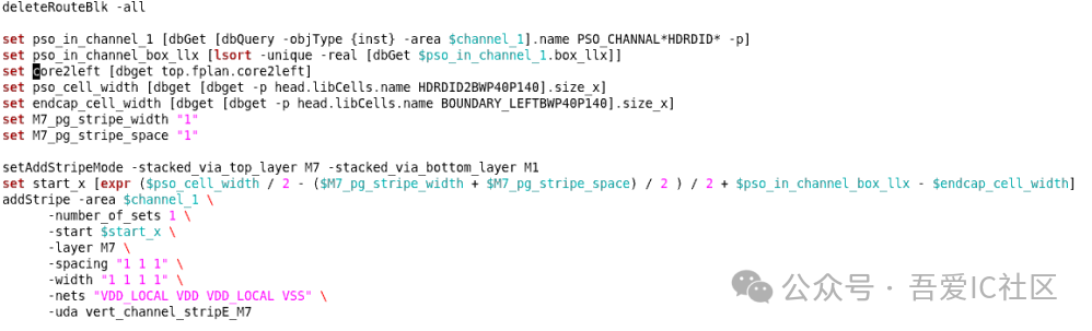
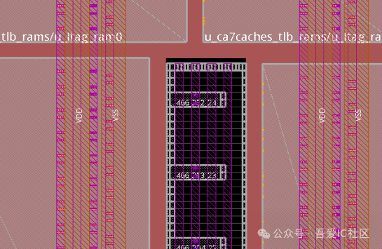
It can be seen that the middle channel area has a set of M7 power stripes, and the result is the same as that of the core area.
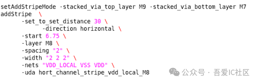
After finishing all five sets of channel power stripes, we also need to add a set of horizontal M8 power stripes to connect the M7 power stripes inside the channel with the M7 power stripes in the core area, while also connecting M9 and M7 through M8 to form a complete top-level power network.
The effect after the addition is shown in the figure below; the horizontal ones are the M8 power stripes.
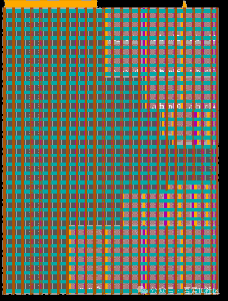
Each M8 is composed of VDD, VSS, and VDD_LOCAL, and then connected to M7 and M9 through vias.
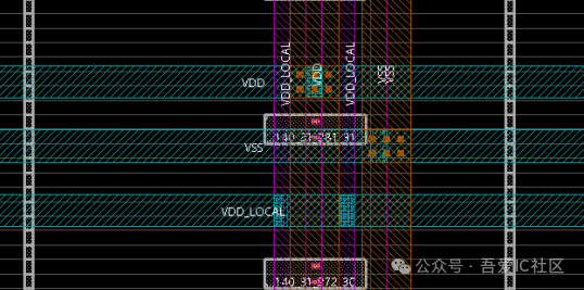
Finally, we connect M1 power rails through sroute, linking M7’s VDD_LOCAL and VSS with M1, thus forming a complete power network.
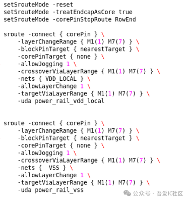
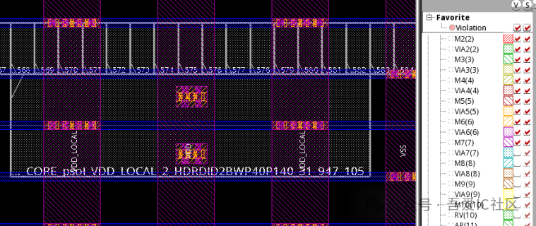
Turning off the layers above M7, it can be seen that both VDD_LOCAL and VSS will connect downwards via vias to M1.
How to chain power switch cells in the memory channel?
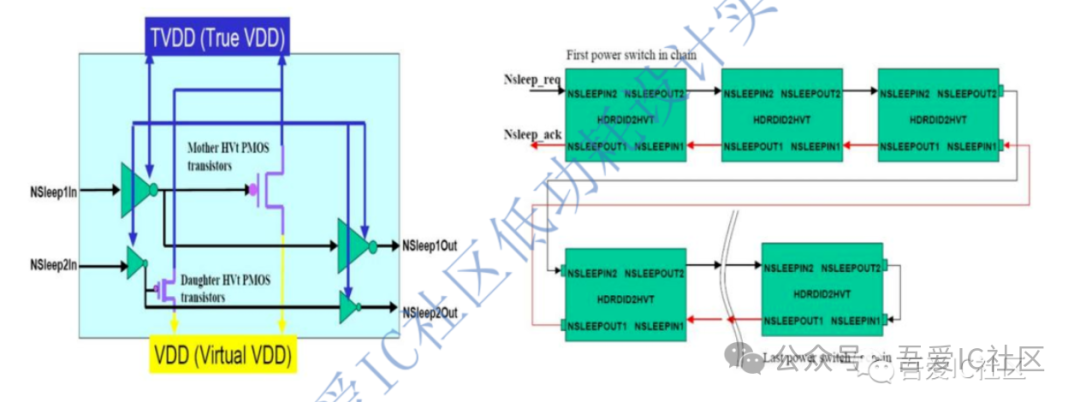
The power switch cell for TSMC28nm has two chains, namely NSleep1 and Nslee2, with Nslee2 being the small chain that should be prioritized. Therefore, the effect of chaining power switch cells is shown on the right side of the figure below, chaining NSleep2 first and then returning to chain Nslee1.
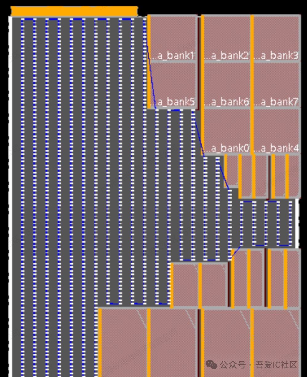
The essence of chaining power switch cells is to find the shortest path among N known points. The effect diagram of chaining in the core area is shown below.
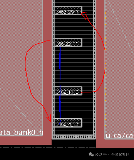
The chaining in the memory channel needs to follow the principle shown in the figure below—alternating chaining. This ensures that the control signals for NSLEEP between each power switch cell are the shortest.
What to do if the power switch chain corresponding net has transitions?
Since the control signals for the PSO switches are static signals, the transition constraints for these nets can be relaxed appropriately. However, if there is indeed a large max transition violation, such as exceeding the threshold, we can use an always-on buffer (AON buffer) to fix the transition.
It should be noted that the AON buffer also has a VDDG global VDD pin, which also needs to be routed as a secondary pg pin.
Power network connectivity and DRC checks
After adding PSO and designing the power plan, the following commands should be used to check the power connectivity and perform DRC checks.
verifyConnectivity -type special -noAntenna -noWeakConnect -noUnroutedNet -error 1000 -warning 50 -net VDD
verifyConnectivity -type special -noAntenna -noWeakConnect -noUnroutedNet -error 1000 -warning 50 -net VDD_LOCAL
verifyConnectivity -type special -noAntenna -noWeakConnect -noUnroutedNet -error 1000 -warning 50 -net VSS
verify_drc
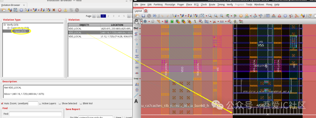
The VDD open violation shown below is something that every student has encountered. Here, everyone should think about why this open occurs and how to avoid this type of violation during the power plan stage.
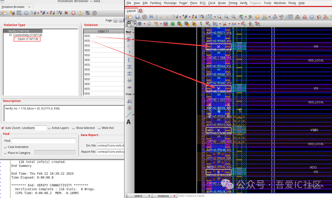
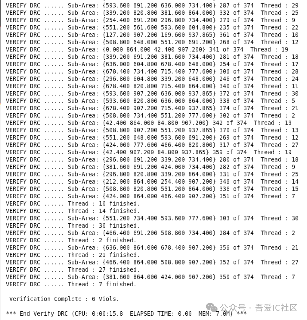
The results of the DRC check are shown in the figure below. Even if Innovus’s DRC results are clean, it does not mean that Calibre signoff’s DRC is clean. Therefore, we recommend that everyone write out the GDS to Calibre for a comprehensive DRC check after completing the floorplan and power plan.
https://alidocs.dingtalk.com/i/nodes/7Y36k14mK9AV3qQ5nXgq85NqapjblR2D?doc_type=wiki_doc&utm_medium=main_vertical&utm_scene=team_space&utm_source=search# “Calibre DRC Comprehensive Analysis and Repair Methods (Training Camp Student Cases)”
Alright, that concludes today’s content sharing. Additionally, due to changes in the public account’s push rules, the valuable content shared by me may not be pushed to everyone in a timely manner. To avoid missing out on exciting content, please follow the star-marked public account, click “View” and like, and share it to your moments, so that the push algorithm knows you are a part of the community, and you won’t miss any exciting content.
If you want to have further communication opportunities with me, welcome to join my Knowledge Planet, let us learn and grow together, and make progress together. I believe that here can help you achieve a better version of yourself.
Introduction to my Knowledge Planet (If you desire progress, expect high salaries, and enjoy communication, welcome to join):
Here, the things that have been planned and are being worked on include:
-
Writing ICC/ICC2 lab
-
Backend implementation process based on ARM CPU
-
Using CCD (Concurrent Clock Data) in ICC to implement high-performance module design
-
Digital backend Hierarchical Flow implementation tutorial based on ARM quad-core CPU
-
Clock tree structure analysis
-
Low power design implementation
Regular technical sharing of problems encountered in projects in case form
-
Digital IC industry encyclopedia
My Love IC Community Knowledge Planet is run by the public account “My Love IC Community” owner, engaged in digital IC backend design implementation work for 12 years, with successful tapeout experience in advanced process nodes such as 55nm, 40nm, 28nm, 22nm, 14nm, successfully tapeout over thirty chips.
This is a knowledge community in the highly vertical and segmented field of digital IC design implementation, the largest and most high-end knowledge exchange and sharing community in the field of digital IC design implementation, gathering countless engineers in digital IC frontend design, backend implementation, and analog layout.
Here, everyone can build connections, communicate, and expand their network, even organize offline activities. You can ask questions about related issues in the field of digital IC backend design implementation, consult on career development planning, or discuss the problems that trouble you. For the questions asked, I will try to answer them; if I encounter something I do not understand, I will consult materials or ask experts to answer them. Everyone is encouraged to actively post topics and ask questions to promote a positive cycle in the entire knowledge community. Every month, I will reward active users.
The most important thing is that here, with the help of this knowledge community, you can achieve the dream of an annual salary of one million within a short period! Whether you believe it or not, those who have already joined certainly believe it! Meeting is a kind of fate, and knowing each other is an even more precious feeling! If we are fated, you and I will definitely meet and know each other! The QR code for Knowledge Planet is below, you can scan or press and hold to identify the QR code to enter. Currently, there are 2799 members in the planet, thanks to these 2799 friends for their support! Welcome all fans eager for progress and high salaries to join! The ultimate goal is to create a grand goal of achieving an annual salary of one million for all members of this knowledge planet.
Please follow “My Love IC Community”
WeChat ID:ic-backend2018