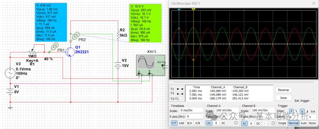
In the Multisim workspace, place two DC voltage sources V1 (5V) and V2 (15V), one AC small signal source V3 (effective value 0.1V, frequency 100Hz), one potentiometer R1 (1MΩ), one resistor R2 (5kΩ), one BJT Q1 (2N2221), two probes PR1 (to measure the base potential current of the BJT) and PR2 (to measure the collector potential current of the BJT), and one dual-trace oscilloscope XSC1 (Channel A observes the waveform of V3 in red, Channel B observes the collector potential waveform of the BJT, which is the output waveform, in green). Connect as shown in the figure below. Since V3 is connected to both V1 and the BJT with wires, it is referred to as directly coupled. The common terminal for the input small signal V3 and the output collector potential waveform is the emitter of the BJT, thus it is called a common emitter amplifier. Adjust R1 to 40% (i.e., the resistance value of R1 connected to the base is 400kΩ).
(1) After starting the simulation, the oscilloscope waveform and probe measurement results are shown in the figure below. From the simulation results, it can be seen that the DC potential at the base of the BJT is 617mV, the DC potential at the collector is 10.1V, the emitter junction is forward biased and conducting, the collector junction is reverse biased, and the BJT is in the amplification state. The DC current amplification factor is 979/11≈89, and the AC current amplification factor β is 58.6/0.699≈83. The DC current at the emitter is 979+11=990uA=0.99mA. The dynamic resistance of the emitter junction of the BJT rbe is approximately 300+(83+1)×26/0.99=2506Ω≈2.5kΩ, and from theoretical derivation, the AC voltage amplification factor of this circuit is Au=(-β×R2)/(400k+2.5k)≈–1.03. Observing the oscilloscope waveform, it can be seen that the output waveform is undistorted and is inverted compared to the input waveform. At time T1, V3 is 140.089mV, and the output waveform Vo is -145.292mV, thus Au=Vo/V3≈–1.037, which is basically consistent with the theoretical estimate.
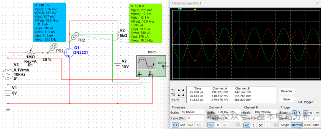
(2) Adjust the frequency of V3 to 10kHz, keeping other parameters unchanged. Start the simulation, and the results are shown in the figure below. From the simulation results, it can be seen that except for the frequency change, other parameters are basically the same as when the frequency of V3 was 100Hz. That is, for the same amplifier circuit, as long as the frequency of the signal source is within a certain range (commonly referred to as the mid-frequency band), the amplification factor remains basically the same. Readers can modify the frequency of V3 themselves to observe its effect on the amplification factor.
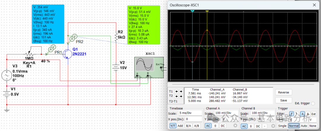
(3)Set V1 to 0.5V, keeping other parameters unchanged. Start the simulation, and the results are shown in the figure below. It can be seen that due to the small value of V1, after superimposing the AC small signal V3, the BJT enters the cutoff region during certain time periods (when V3 is in the negative half-cycle), and the output waveform exhibits cutoff distortion (the upper half of the green waveform is flattened). Readers can adjust other parameters to observe their effect on the working waveform.
Directly coupled common emitter amplifier circuits have a simple structure, but the amplification factor is relatively small, and the negative terminal of the AC small signal V3 is not grounded, resulting in poor anti-interference capability of the circuit, and the internal resistance of V3 (not marked in the simulation circuit) can pass DC current, leading to higher power consumption. In practice, fixed biasing with capacitor-resistor coupling is commonly used for common emitter amplifiers to amplify AC small signals.