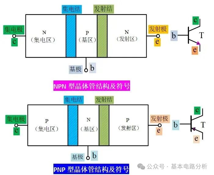
The bipolar junction transistor, also known as a transistor or BJT, is a core component in analog circuits. It can be classified into NPN and PNP types based on structure; silicon and germanium types based on material; low-frequency, high-frequency, and ultra-high-frequency types based on operating frequency; and small, medium, and large power types based on allowable power dissipation. An NPN-type BJT is formed by sandwiching a layer of P-type semiconductor between two layers of N-type semiconductor, while a PNP-type BJT is formed by sandwiching a layer of N-type semiconductor between two layers of P-type semiconductor. The three layers of doped semiconductors are the emitter region, base region, and collector region, each connected to an electrode: the emitter (e), base (b), and collector (c). The PN junction between the emitter region and base region is called the emitter junction, and the PN junction between the collector region and base region is called the collector junction. The structure and symbol of the BJT are shown in the figure below, with the arrow in the symbol indicating the direction of the emitter current.
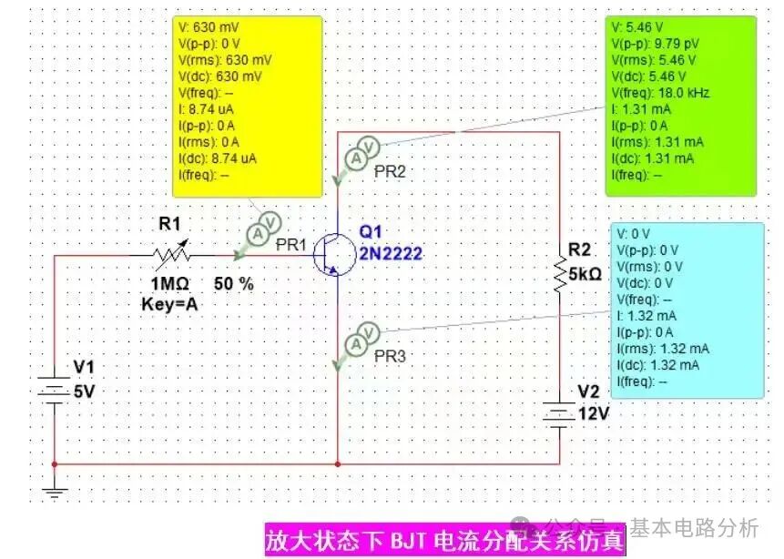
From the structure of the BJT, it appears that the two N regions (or two P regions) are symmetrical, but they have specific manufacturing characteristics: (1) The doping concentration in the emitter region is much greater than that in the collector region, meaning the majority carrier concentration in the emitter region is very high. (2) The base region must be made very thin and have a low concentration, typically a few micrometers to tens of micrometers thick. (3) The collector region has a relatively large area. Thus, the collector region of the BJT is not completely symmetrical with the emitter region, and the collector and emitter cannot be interchanged during use. There are many manufacturers of BJTs worldwide, and numerous models are available; readers can refer to BJT manuals as needed. In the Multisim workspace, place one DC voltage source V1 (5V), one DC voltage source V2 (12V), one variable resistor R1 (1MΩ), one BJT Q1 (2N2222 from the USA, with β approximately 150 at room temperature), one resistor R2 (5kΩ), and three probes PR1, PR2, and PR3 to measure the potentials and currents at the base, collector, and emitter, respectively, as shown in the diagram below. (1) Set R1 to 50%, start the simulation, and find that probe PR1 indicates the BJT base DC potential VB=630mV, base DC current IB=8.74uA; PR2 indicates the BJT collector DC potential VC=5.46V, collector DC current IC=1.31mA; PR3 indicates the BJT emitter DC potential VE=0V, emitter DC current IE=1.32mA. It can be seen that VBE=0.63V (emitter junction forward-biased), VBC=0.63-5.46=-4.83 (collector junction reverse-biased), and the BJT operates in the amplification state, at which point IC/IB=1.31/0.00874=149.88≈150=β, and IE≈IB+IC.
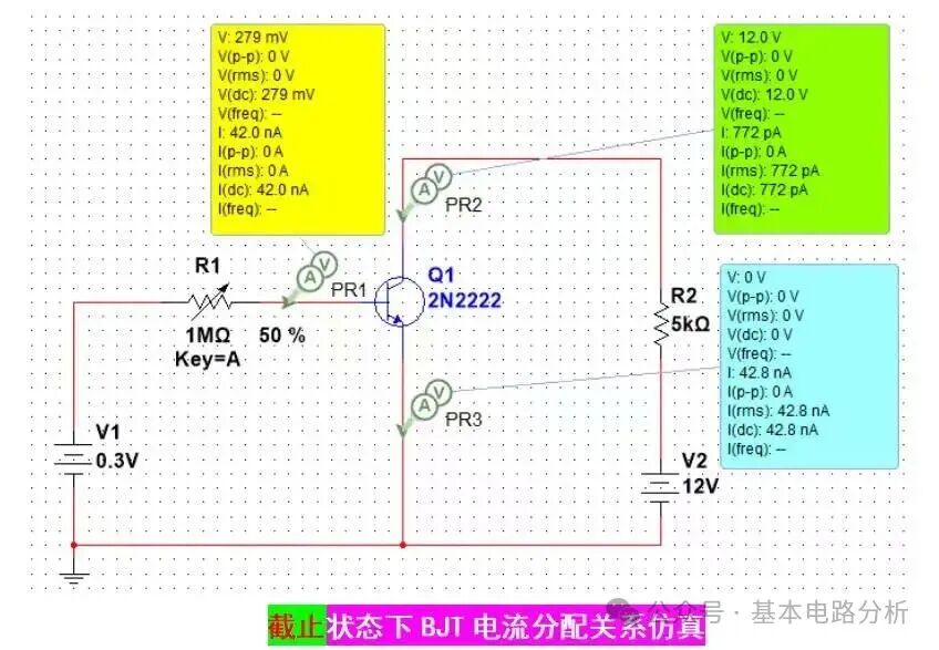
(2) Change V1 to 0.3V, keeping other parameters the same as in the amplification state. Start the simulation and find VB=279mV, IB=42.0nA (approximately 0); VC=12V, IC=772pA (approximately 0); VE=0V, IE=42.8nA (approximately 0). When V1=0.3V, the BJT emitter junction fails to be forward-biased and remains in the cutoff state, with each electrode’s current approximately 0mA.
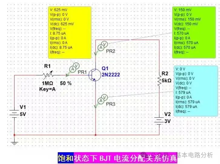
(3) Change V2 to 3V, keeping other parameters the same as in the amplification state. Start the simulation and find VB=625mV, IB=8.75uA; VC=150mV (very small), IC=570uA; VE=0V, IE=579uA. When V2=3V, although the BJT emitter junction can be forward-biased, V2 is too small to reverse-bias the collector junction, causing the BJT to operate in saturation state. Although IE≈IB+IC, IC/IB=570/8.75≈65, which is far less than β=150, indicating that the BJT’s current amplification capability is weak. Readers can modify other parameters to observe their effects on the BJT’s operating state.