
This series will bring systematic learning of FPGA, starting from the most basic digital circuit fundamentals, with the most detailed operational steps and straightforward descriptions, providing a hand-holding “fool-proof” explanation, allowing students in electronics, information, and communications, as well as newcomers to the workplace and career developers looking to advance, to have the opportunity for systematic learning.
Systematically mastering technology development and related requirements can potentially help personal employment and career development. We hope this will be helpful to everyone. We will continue to update content related to the development of Xilinx’s Vivado, ISE, and related software, and while learning FPGA design methods and design concepts, combining practical operations with various software will make your journey in technical learning incredibly smooth, bidding farewell to technical learning bugs and misleading training. Without further ado, let’s get started.
Signal Tap Logic Analyzer User Guide
Author: Xu Shuai Hao Proofreader: Hui Lu
In previous design development, data from a certain unit was obtained using ModelSim, and the inputs were also provided by the designer in the testbench. However, in practical applications, the external input signals may not match those described in the testbench, which could lead to successful RTL simulation but failed board tests.
The Signal Tap Logic Analyzer captures and displays real-time signal behavior in FPGA designs, allowing for the inspection of internal signal behavior during normal device operation without additional I/O pins or external laboratory equipment.

During data acquisition, the memory module in the device stores the captured data, which is then transmitted to the logic analyzer via a JTAG communication cable.
The following diagram illustrates the task flow of the Signal Tap Logic Analyzer.

-
Design Requirements
Use the logic analyzer to measure the width of each bit time when the computer sends UART (at a baud rate of 115200).
-
Design Analysis
The UART protocol specifies that the width of each bit should be 1 second divided by the baud rate, but in actual circuits, two oscillators with the same label may have some discrepancies. We can use the logic analyzer (i.e., using the FPGA’s clock) to measure the bit time width when the PC sends UART.
Since the baud rate is 115200, a 16x oversampling is generally used. At this time, the sampling frequency is relatively high, and a basic 50MHz clock cannot achieve accurate 16x oversampling, which also brings some errors.
The logic analyzer allows us to see the actual sampling deviations in the above two cases, as well as whether these deviations affect our design.
-
Design Implementation
Copy _9_uart_drive and rename it to _10_uart_drive_signal_tap. Then open this project and change the baud rate to 115200.
Click tools -> Signal Tap Logic Analyzer.


In the right window of signal configuration, you first need to specify a sampling clock signal.

The logic analyzer samples data on each rising edge of the sampling clock. The logic analyzer does not support sampling on the falling edge of the sampling clock. Any signal in the design can be used as the sampling clock. However, for the best data sampling results, please use a global clock synchronized with the signal being measured.
In this design, all signals are driven by an external clk signal, so this sampling clock is selected as clk. After clicking the clock dialog box, click the three dots behind it. Set the filter to pin: all, click list, select clk in matching nodes, click “greater than”, and clk will appear in nodes found, then click ok.


After configuring the sampling clock signal, you need to configure the sampling depth.
For each signal in the sampled data, the sampling depth specifies the number of samples to be taken and stored. In cases where the device’s memory resources are limited, if the selected depth is too large, the design may not compile. At this time, you need to reduce the sampling depth to decrease resource usage.
The sampling depth multiplied by the sampling interval determines the sampling time width. Now we want to sample a UART protocol frame, which consists of 12 bits. According to the baud rate of 115200, the sampling time width should be 104166ns, so the sampling depth should be 5208; here we choose a sampling depth of 8K.

Once the sampling depth is determined, you can specify the amount of data the logic analyzer samples before and after the trigger event.
The logic analyzer provides three options. Pre means that 12% of the storage depth is used for before the trigger event, and 88% for after; Center means 50% for before and 50% for after; Post means 88% for before and 12% for after the trigger event.
Here, we choose Pre.

After configuring this information, start adding the signals you want to observe.
In the setup interface, double-click on the blank area to add the signals you want to observe.

The signals to be observed are uart_txd, uart_rxd, cap_cnt.
uart_txd and uart_rxd are port signals; when selecting a filter, choose PIN: all. cap_cnt is an internal signal; when selecting a filter, choose signal tap: pre-synthesis.

Set the falling edge of uart_rxd as the trigger condition.
Right-click on the trigger conditions for uart_rxd and select falling edge.


Click save, save to qprj, and name it stp1.stp.
Enable the logic analyzer. Click Yes.

Return to the Quartus interface, perform synthesis analysis, and generate the configuration file.
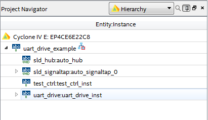
In the project wizard’s structure interface, you can see two unknown components appearing in the structure. These two are the logic analyzers.
In the report, you can see that the logic resources and memory resources used have increased.

Return to the Signal Tap interface and connect the PC and development board.
In hardware, select USB – blaster.

Click the three small dots behind sof manager, select the generated sof file, and then click download.

Click to run the analysis.

At this point, the logic analyzer is waiting to be triggered.

The trigger condition is the falling edge of uart_rxd. Open the serial port assistant, configure it, and send a data byte of 11.

After sending, the waveform appears in the logic analyzer. Since 11 is sent, the first data should be 1, so the first low level is the start bit. The time width can be determined using the sampled digital number.

Left-click to zoom in, right-click to zoom out.
The left side is 0 because the falling edge is used as the trigger condition. Zooming in on the left side gives 434.

Thus, the time width of the start bit is 434x20ns, which equals 8680ns. According to the baud rate of 115200, the time width of each bit should be 8680.5556ns. This confirms that the bit time width sent from the PC is consistent with our expectations.
This method can be used to measure the width of other bits; some bits may be less than 8680ns, while others may be more, but the deviations are similar.
Since there is a certain difference between the actual width and our assumed width, the design is based on each bit width being an integer multiple of 20ns, which leads to deviations during sampling. This can be observed through cap_cnt, and as the sampling length increases, the error will accumulate.
At the first bit of the data, cap_cnt equals 7 and will soon change to 8. According to the counting rule of cap_cnt, it is designed for 16x frequency, so all subsequent bit starts should be 16 *N + 7 and then quickly change to 16 * N + 8. However, there is a certain deviation between the actual time width and the expected time width.

At the start of the last parity bit, the data of cap_cnt should equal 135 according to the 16x frequency sampling, and it should quickly change to 136. However, it is already equal to 136 at this point and quickly changes to 137.
We sample based on cap_cnt (sampling at the position where cap_cnt changes).
Due to the error, it is stipulated that the length of the UART protocol frame cannot be too long, meaning the number of data bits in between cannot be arbitrarily increased.
The numerical results from the above analysis steps are only the author’s test results, and different PCs and development boards may yield different results during testing.
-
Logic Analyzer Summary
The logic analyzer allows you to directly view the waveforms running inside the development board. Therefore, it is often used for board-level testing as the final result.
If the logic analyzer is not needed in the project, you can go to assignments -> settings -> signal tap logic analyzer, uncheck the enable box, and recompile.


– End –
Previous Recommendations
-
Quartus Prime 18.0 Standard Edition Installation and Crack Process Explanation
-
The Most Practical ModelSim Beginner’s Tutorial
-
Digital Electronic Technology Basics (6th Edition) Textbook Yan Shi Electronic Version


Scan the QR code for more exciting content
