
Click the blue text to follow us
Follow and star our public account for exciting content delivered daily

Source: Online Materials
1 Reasons for Changing FPGA Debugging Technology
During the functional debugging of hardware design, the reprogrammability of FPGAs is a key advantage. In the early use of CPLDs and FPGAs, if a design was found to be malfunctioning, engineers used the “debug hook” method. They would first route the internal signals of the FPGA to pins, then use an external logic analyzer to capture the data. However, as the complexity of designs has increased, this method has become unsuitable for several reasons. The first is that while the functionality of FPGAs has increased, the number of pins on the devices has grown slowly. Thus, the ratio of available logic to I/O has decreased, as seen in Figure 1. Moreover, when designs are complex, there are often only a few spare pins left after the design is completed, or there may be no spare pins available for debugging at all.
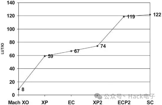
Figure 1 LUT/Available I/O of Lattice FPGA
Secondly, the complexity of current designs often requires monitoring many signals rather than just a few. A common technique is to implement a wider internal bus to achieve high system throughput in larger FPGAs. If there is suspicion of bad data on an internal 32-bit bus, it is difficult to pinpoint the problem using just a few I/O pins.
Thirdly, it is often necessary to test complex functionality within the system. In such cases, access to some I/O during system debugging may be limited. New types of packages also restrict access to FPGA pins. System speed is also an issue, as the connection of probes may lead to performance degradation or noise signals.
Finally, a key factor driving the change in FPGA debugging methods is the advent of new tools that utilize internal or embedded logic analyzers.
Having these tools can yield optimal results, rather than using the same methods as previous tools. Resources, static parameters, and dynamic parameters typically constrain both internal logic analyzers and external logic analyzers. This article compares the constraints of these two types of tools and examines how to best utilize internal logic analyzers.
2 Limitations of External Logic Analyzers
External logic analyzers have been in use for decades. The biggest advantage of external logic analyzers is their ability to store a large amount of signal information or track data. Configurations are constantly changing, but most external logic analyzers can store megabytes of data. To use an external logic analyzer with an FPGA, data signals must be routed off-chip. This can be done using one of two methods. The first method is to directly send signals to the I/O pins used for observation. Depending on the packaging type of the FPGA, accessing the I/O pins may be difficult. Circuit board designs for debugging using this method need connectors, such as MICTOR connectors connected to the FPGA. However, this method is not very effective because each signal requires an I/O pin.
The second method is to insert cores that can route the signals to the I/O. The advantage of this method is that the core is designed to multiplex signals to I/O pins, allowing pin sharing. The limitation of this method is that signals must be captured in real-time by the external logic analyzer, and multiplexing significantly reduces the chances of quickly capturing signals. For this reason, 2x or 4x multiplexing schemes are typically used. This means that now 32 I/O pins can support 64 or 128 signals. This results in a significant improvement, but there are still limitations, such as debugging wide buses. Once signals are connected to the external logic analyzer, trigger and data capture conditions are then set.
The constraints of using external logic analyzers include limited signals, high-speed trigger logic, and a large amount of tracking memory. Most logic analyzers use state machine triggering mechanisms. The user specifies a value to wait for this signal, then captures the data, or transitions to another state to look for different conditions. These signals themselves are static, but various conditions are dynamic and can change at any time. Given the constraints, this method is very effective. Because the number of signals is limited, the number of operations is reduced in the case of signal combinations. However, tracking memory is relatively large, and it is common to try to find a close observation point and then capture a large amount of data to find the problem.
3 Using Internal Logic Analyzers
Using internal logic analyzers can debug FPGA functionality just like external logic analyzers. Internal logic analyzers use one or more logic analyzer cores embedded in the FPGA design. Designers set trigger conditions in software on a PC and access the FPGA through JTAG. Once the logic analyzer soft core captures the data, it returns the information to the PC via JTAG, where the designer can then observe this data. The complexity of the trigger signals and the size of the tracking memory limit the number of signals. In most cases, designers can observe hundreds or thousands of signals.
Trigger resources are constrained by the FPGA, namely the unused logic and RAM. Some implementations of tracking memory require RAM. Some require either RAM or LUT. However, the required tracking memory is significantly reduced compared to using external logic analyzers, typically in the order of thousands of bits versus millions of bits. Triggering and data capture occur at full design speed because signals do not need to be multiplexed off-chip.
With external logic analyzers, signals must be statically defined. Changing signals often requires the FPGA to run again, although some tools provide the capability to change part or all of the connected signals by only adding FPGA wiring. During debugging, most implementations dynamically change part or all of the trigger conditions. However, the change in trigger complexity depends on the tools used. The more different the signals, the smaller the memory that can be provided. To achieve optimal results, different triggering options drive the need to use internal logic analyzers.
An example of complex debugging is finding a particular pixel in SMPTE SDI HD displays. In special cases, finding the EAV (end active video) timing is necessary, then finding the specific line number associated with the data, and finally finding the SAV (start active video) timing. Finally, based on the corresponding pixel in the line, the number of bytes is calculated, see Figure 2.
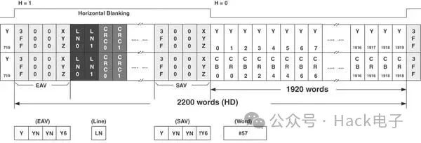
Figure 2 Example of SDI HD Data Stream
To debug and find such data requires looking for timing of values, then finding special values, and finally counting the number of clocks before capturing data. To understand how this is done, one must look at the specific implementation process. Lattice’s Reveal hardware debugger uses trigger units and trigger representations to determine trigger points. The trigger unit is a comparator, and the trigger representation allows the trigger unit and sequence values to be combined.
For this SDI example, three trigger units are used to define the EAV and SAV sequences, with another trigger unit for the line number, and finally a counting statement before discovering data to wait for. The example of the established trigger is shown in Figure 3. This setup can be used to find any required line number and pixel, as the triggered values and counts for line numbers can be dynamically changed.
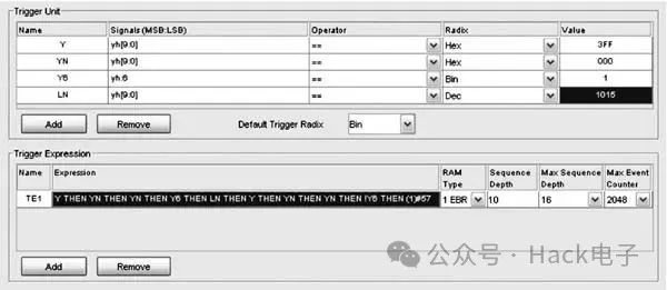
Figure 3 Example of Trigger Setup
4 Conclusion
Engineers will continue to use external logic analyzers because they are very valuable for analyzing system-level functionality. However, the number of signals is limited when using them for internal FPGA debugging, which requires connection to the circuit board. In contrast, internal logic analyzers provide great freedom in the number of available signals, but are constrained in terms of trigger logic and tracking memory. However, careful use of triggering options allows internal logic analyzers to start capturing data at precise times, maximizing the available resources. In this example, the complex implementation of analyzing special pixels (lines and bytes) in SDI video signals is broken down into simpler elements, which improves efficiency. This example only skimmed the use and application of internal logic analyzers. As the complexity of FPGA designs continues to increase, internal logic analyzers and similar tools are favored by designers for functional verification and debugging.

Want to learn about FPGA? Here are example shares, ZYNQ design, follow our public account to explore