
Concept of Logic Analysis
The logic analyzer is also a very commonly used instrument, just like the oscilloscope, and is one of the classic instruments for digital design and measurement. When measuring digital circuits, when should an oscilloscope be used? Generally, an oscilloscope can be used when precise parameter information (such as time intervals and voltage readings) is needed. Specifically:
-
When measuring small voltage offsets of signals (such as below or above).
-
When high time interval precision is required. An oscilloscope can collect precise parameter information, such as the high precision time between two points on the rising edge of a pulse.
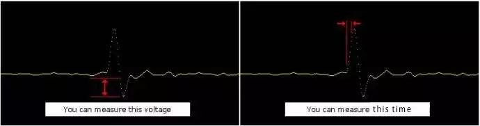 Figure 1 Oscilloscope used to measure the analog waveform of a signal
Generally, a logic analyzer is used to observe the timing relationships between multiple signals or to capture the data carried by the signals. When the signal from the device under test exceeds the voltage threshold, the logic analyzer will respond similarly to the logic circuit. It will identify the high and low of the signal. Specifically:
-
When there is a need to immediately view multiple signals. The logic analyzer can well organize and display multiple signals. A typical task is to group multiple signals into a bus and assign a custom name. Address, data, and control buses are representative examples.
-
When signals in the system need to be viewed in the same way as hardware. Signals are displayed on a timeline, allowing the occurrence time of transitions relative to other bus signals or clock signals to be viewed.
-
When information in the bus needs to be captured based on clock edges, similar to a receiving chip. The receiving chip determines the address, command, and data on the bus based on clock edges. The logic analyzer acts like a listener, capturing the information transmitted on the bus and storing the necessary information in memory. Trigger conditions can be set to capture information on the bus that needs attention or is problematic, which can help understand the status of protocols or software execution.
We have briefly discussed some uses of logic analyzers above; now, let’s delve into the concept of logic analyzers in more detail. So far, we have widely used the term “logic analyzer”. In fact, most logic analyzers contain two types of analyzers.
1. Timing Analyzer:
The timing analyzer is part of the logic analyzer, and it is similar to an oscilloscope. In fact, their relationship is very close. The general form of information displayed by the timing analyzer is the same as that of an oscilloscope, where the horizontal axis represents time and the vertical axis represents voltage amplitude. Since the waveforms on both instruments depend on time, this display can be said to be in the “time domain”.
2. State Analyzer:
The state analyzer is very suitable for tracking defects in software or faulty components in hardware. It helps determine whether the problem lies in the software code or in certain hardware devices. In most cases, the state analyzer is used to find out what logic levels exist on the bus when a specific clock signal occurs. In other words, it can understand what “active states” will be displayed when the clock appears and assuming data is valid. The data collected in memory will be displayed in a list format, with time tags connected to each state.
Timing Analysis
The timing analyzer uses its own internal clock to control data sampling. This type of clock timing makes the data sampling in the logic analyzer asynchronous with the clock in the device under test. Specifically:
-
The timing analyzer is suitable for displaying when signal activity occurs “relative to other signals”.
-
The timing analyzer focuses on viewing the timing relationships between individual signals, rather than the timing relationships with signals controlled by the device under test.
-
This is why the timing analyzer can sample data that is “asynchronous” or out of sync with the clock signal of the device under test.
In timing acquisition mode, the logic analyzer works by sampling the input waveforms to determine whether they are high or low. To determine the high and low levels, the logic analyzer compares the voltage levels of the input signals with a user-defined voltage threshold. If the signal is above the threshold at the time of sampling, the analyzer displays the signal as 1 or high. Similarly, signals below the threshold will be displayed as 0 or low. The following diagram illustrates the sampling of a sine wave by the logic analyzer when it crosses the threshold level.
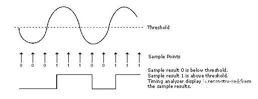
Figure 2 Principle of timing analysis acquisition
After acquisition, the sampled points are stored in memory and used to reconstruct square digital waveforms. This process of making everything square seems to limit the use of the timing analyzer. However, the timing analyzer was never intended to be used as a parameter instrument. To view the rise time of a signal, an oscilloscope can be used. If you need to check the timing relationships between several or hundreds of signals simultaneously, then the timing analyzer is the right choice.
When the timing analyzer samples the input channels, the channel signal is either high or low. If the channel is in one state (high or low) at the time of one sampling, and changes to the opposite state at the next sampling, the analyzer can “know” that a transition has occurred at some point between these two samples. However, it does not know exactly when, so it places the transition point at the later sample, as shown in the following diagram.
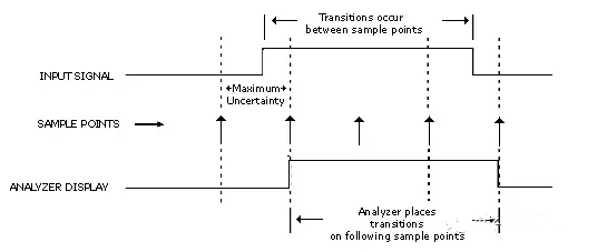
Figure 3 Sampling accuracy (uncertainty) of timing analysis
There is a certain ambiguity regarding when the transition actually occurs and when the analyzer shows the transition. If the transition occurs immediately after the previous sampling point, this uncertainty is at most one sampling period. However, for this method, there is also a trade-off between accuracy and total sampling time. Remember that each sampling point only uses one storage location. Therefore, the higher the accuracy (the higher the sampling frequency), the shorter the sampling period.
Triggering the Timing Analyzer:
At certain points in the measurement, the logic analyzer must know when to collect (store) the data flowing through its memory. These points are called trigger points.
One way to trigger the analyzer is to configure it to look for specific upper or lower code patterns from a set of signals (bus) or to look for rising or falling clock edges of a single signal. When the analyzer finds the specified code pattern or clock edge in the data, it triggers.
Pattern Trigger:
Pattern trigger is used to look for specific upper and lower code patterns on the bus. You can specify different criteria, such as equal to, not equal to, within or outside a certain range, or greater than/less than.
Example: A bus containing 8 signal lines is configured with simple trigger to specify that the analyzer triggers when the input data equals the “AA” code pattern.
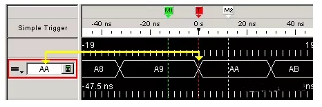 Figure 4 Pattern Trigger
To facilitate use for some users, most analyzers allow trigger points to be set not only in hexadecimal but also in binary (1 and 0), octal, ASCII, or decimal. For example, the hexadecimal trigger value AA can also be set to the equivalent binary trigger value 1010 1010. However, it is especially helpful to set trigger points in hexadecimal when looking for 16, 24, 32, or 64-bit wide buses.
Clock Edge Trigger:
Clock edge trigger is a familiar concept for users accustomed to using oscilloscopes. Adjusting the “trigger level” knob on the oscilloscope can be seen as setting the level of a voltage comparator: when the input voltage exceeds that level, the voltage comparator informs the oscilloscope to trigger. The clock edge trigger of the timing analyzer is generally similar, except that the trigger level is pre-set to a logical threshold.
Many logic devices rely on levels, and the clock and control signals of these devices are often affected by clock edges. Through clock edge triggering, data collection can begin while timing the device.
Example: Imagine a clock edge-triggered shift register that does not correctly shift data. Is the data problematic or is the clock edge problematic? To detect the device, we need to check the data while timing it (based on clock edges). The analyzer can be instructed to collect data when a clock edge occurs (either rising or falling) and capture all outputs of the shift register.
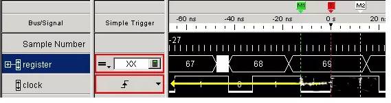 Figure 5 Edge Trigger
Transitional Timing:
In Transitional / Store qualified (transitional/store qualified) timing mode, the timing analyzer will periodically sample data, but will only store data when there is a signal transition present in the threshold voltage level. Whenever any bit in the defined bus/signal (not excluded) transitions, data from all channels is stored. A time tag is stored for each stored data sample, allowing reconstruction and display of the measurement later.
Typically, transitions do not occur at each sampling point. The following will illustrate with time tags 2, 5, 7, and 14. When a transition does occur, two samples are stored for each transition. Therefore, storing 1K transitions will result in 2K memory samples. One transition necessary for the starting point must be removed to ensure that the minimum transition count stored reaches 1023.
If transitions occur rapidly, such as one transition at each sampling point, then as shown by time tags 17 to 21 in the figure below, only one sample is stored for each transition. If the entire tracking process remains this way, the number of stored transitions will be 2K samples. Additionally, one starting point sample must be removed to ensure that the maximum transition count stored does not exceed 2047.
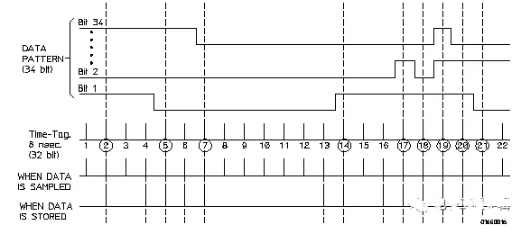 Figure 6 Data storage during transitional timing
In most cases, transitions are tracked and stored when both minimum and maximum transition counts are present. Therefore, in this example, the actual transition count stored will be between 1023 and 2047.
Considerations for Transitional Timing:
When a clock edge is detected, two samples are stored across all channels assigned to the timing analyzer. If a second clock edge occurs before the timing detector resets (after the first clock edge), two samples are needed to avoid data loss.
In transitional timing, each sequence step has only 2 branches. In transitional timing, only one global counter is available.
Transitional timing requires time tags to reconstruct data. Time tags can be stored by cross-referencing them with the measurement data in memory.
By default, the analyzer will look for transitions on all buses/signals defined for the logic analyzer module. However, to increase the available memory depth and acquisition time, certain bus/signal transitions can be excluded from storage in advanced triggering (e.g., adding unnecessary information to the measurement from the clock or gating pulse signals).
During measurement operation, data will be collected on all these channels, regardless of whether the bus/signal is defined or allocated to the logic analyzer channel. In transitional timing mode, if transitions occur on the defined bus/signal (not excluded), the collected samples will be saved.
After running a transitional timing measurement, if new buses/signals are defined for previously unallocated logic analyzer channels, the data collected on these channels will be displayed, but it will not be possible to store all transitions on these buses/signals; the displayed data appears as if the new buses/signals were excluded before running the measurement.
In transitional timing, there is no need to pre-store data (samples obtained before triggering). Therefore, similar to the state mode, the trigger position (start/center/end) indicates the percentage of samples occupying memory after triggering. The number of samples obtained/displayed before triggering will vary across different measurements.
State Analysis
The state analyzer requires a sampling clock signal from the device under test. This type of clock timing allows the data sampling in the logic analyzer to be synchronized with the timing events in the device under test. Specifically:
-
The state analyzer is suitable for displaying what signal activity occurs during the “valid clock or control signal” period.
-
The state analyzer focuses on viewing signal activity within a specified execution time, rather than signal activity that is unrelated to timing.
-
This is why the state analyzer needs to sample data that is “synchronized” or in sync with the clock signal of the device under test.
For microprocessors, data and addresses can appear on the same signal line. To collect the correct data, the logic analyzer must restrict data sampling to only occur when the required data is valid and present on the signal line. To achieve this, it samples data from the same signal line but uses a different sampling clock from the device under test.
Example: The following timing diagram indicates that to collect the address, the analyzer needs to sample when the MREQ line goes low. To collect data, the analyzer needs to sample when the WR line goes low (write cycle) or the RD line goes low (read cycle).
Triggering the State Analyzer:
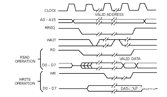
Figure 7 State Acquisition
Similar to the timing analyzer, the state analyzer also has the capability to restrict data that is stored. If we are looking for specific upper and lower code patterns on the address bus, we can notify the analyzer to start storing when it finds that code pattern, and it will continue to store as long as the analyzer’s memory is not full.
Simple Trigger Example:
Consider the “D” flip-flop shown below; the data on the “D” input is invalid before the positive clock edge occurs. Therefore, the state of the flip-flop is valid only when the clock input is high.
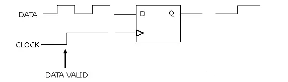 Figure 8 D Flip-Flop
Now, suppose we have eight such flip-flops in parallel. As shown below, all eight flip-flops are connected to the same clock signal.
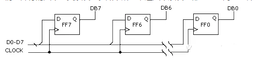 Figure 9 Receiver
When a high level appears on the clock line, all eight flip-flops will sample data at their “D” inputs. Additionally, a valid state will occur every time a positive level appears on the clock line. The following simple trigger indicates that the analyzer collects data on D0 – D7 when a high level appears on the clock line.
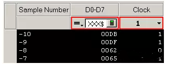 Figure 10 Data collected on the bus
Advanced Trigger Example:
Suppose you want to see what data is stored in memory when the address value is 406F6. Configure the advanced trigger to look for the code pattern 406F6 (hexadecimal) on the address bus and look for a high level on the RD (memory read) clock line.
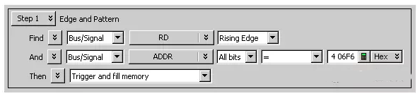
Figure 11 Advanced Trigger Settings
When configuring the Edge And Pattern trigger dialog, try to view the operation as constructing a sentence read from left to right.
Pod, Channel, and Time Tag StoragePod and Channel Naming Conventions:
A pod is a combination of a set of logic analyzer channels, totaling 17 channels, including 16 data channels and 1 clock channel. The number of channels in a logic analyzer is a multiple of the number of pods. A 34-channel logic analyzer corresponds to two pods, a 68-channel logic analyzer corresponds to four pods, and a 136-channel logic analyzer corresponds to eight pods.
For modular logic analyzers (also known as logic analysis systems), taking the 16900 series logic analysis system as an example, the correspondence is as follows:
Slots are named from top to bottom with letters A to F.
A cable labeled Pod 2 connects to each logic analyzer module. It is important to know which pod is connected to which slot because if there are logic analyzer modules in both slots A and B, there will be two cables labeled Pod 2, but the operating interface application will label one as Slot A Pod 2 and the other as Slot B Pod 2. It is important to distinguish between these two cables.
Slot A Pod 2 is equivalent to Pod A2. A2 can be used interchangeably with Slot A Pod 2; similarly, D1 can be used interchangeably with Slot D Pod 1.
The Clock Pod consists of all clock channels from all pods in the module.
Each pod has one clock channel. All clock channels are numbered as Clk1, Clk2, Clk3, etc. If a logic analyzer module has two logic analyzer cards, each with four pods, the clock channels of that logic analyzer will be labeled Clk1 to Clk8.
Besides Clk1, clock channels can also be labeled as C1. C1 and Clk1 are the same.
In the 16900 series logic analysis system, do not confuse the clock channel C2 with Pod 2 in Slot C, which is labeled as Pod C2. For clock channels, C is an abbreviation for Clock, not Slot C.
Why Do Pods Sometimes Go Missing?
There are various reasons why all pods may be unavailable for the logic analyzer module:
-
In state sampling mode, when the general state mode sampling option is selected, selecting maximum acquisition memory depth requires one pod pair to be reserved for time tag storage. In this case, setting the memory depth to half (or less) of the maximum will return the pod.
-
In state sampling mode, when the high-speed state mode sampling option is selected, one pod pair will be reserved for time tag storage.
-
In timing sampling mode, when the transitional/store qualified timing mode sampling option is selected:
-
Selecting the minimum sampling period will reserve one pod pair for time tag storage.
-
Selecting a sampling period other than the minimum requires that one pod pair be reserved for time tag storage when selecting maximum acquisition memory depth. In this case, setting the memory depth to half (or less) of the maximum will return the pod.
-
-
The module is part of a separated logic analyzer. In this case, the pod is located in the other half module of the separated analyzer.
Interrelationships between the number of channels, memory depth, and triggering in state mode and transitional timing mode:
In state sampling mode, time tag storage requires 1 pod or 1/2 of the acquisition memory.
-
In the operating interface application, all modules are time-related; time tag storage cannot be turned off (although previous Agilent logic analysis systems could).
-
To use more than 1/2 of the module’s acquisition memory, one Pod must be reserved for time tag storage. To use all pods, memory usage cannot exceed 1/2 of the module’s acquisition memory.
-
Generally, the number of available timers is the same as the number of pods that are not reserved for time tag storage.
Default Settings:
-
Time tag storage is always on (and cannot be turned off).
-
Memory depth is set to 1/2 of the total acquisition memory.
-
All pod pairs are available for data acquisition.
-
If the entire memory is selected, the default pod for time tag storage is the leftmost pod pair, but any pod that has not been allocated to a bus or signal is available for use.
In transitional timing mode, time tag storage requires 1 pod or 1/2 of the acquisition memory:
-
Transitional timing sampling mode also requires time tag storage.
-
When selecting the minimum sampling period, one pod pair must be reserved for time tag storage. In this case, 1/2 (or less) of the module’s acquisition memory cannot be used as a substitute for that pod.
-
For other sampling periods, the trade-offs between memory depth and channel numbers are the same as in state sampling mode. That is, to use more than 1/2 of the module’s acquisition memory, one Pod must be reserved for time tag storage. To use all pods, memory usage cannot exceed 1/2 of the module’s acquisition memory.
-
Generally, the number of available timers is the same as the number of pods that are not reserved for time tag storage.
Sampling Locations, Eye Positioning, and Eye Pattern Scanning in State Mode
Synchronizing sampling (state mode) logic analyzers with triggering clock edges is similar, as both require input logic signals to stabilize for a period of time before (setup time) and after (hold time) the clock event to correctly interpret logic levels. The combined setup and hold time is called the setup/hold window.
The device under test can specify that data is valid on the bus for a certain period of time due to its own setup/hold requirements. This is called the data valid window. Generally, the data valid window on most buses is less than half of the bus time period.
To accurately collect data on the bus, the following conditions must be met:
-
The setup/hold time of the logic analyzer must be within the data valid window.
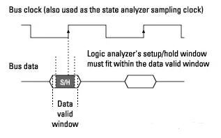 Figure 12 Valid Acquisition Window
 -
Since the location of the data valid window relative to the bus clock varies depending on the bus type, the position of the logic analyzer’s setup/hold window within the data valid window must be adjustable (relative to the sampling clock and with high resolution). For example:
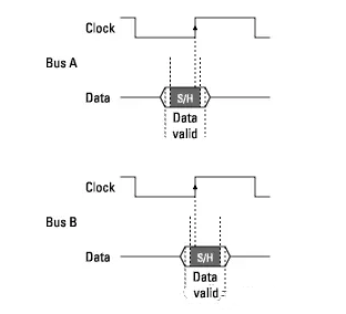 Figure 13 Adjusting Sampling Position
To place the setup/hold window (sampling position) within the data valid window, the logic analyzer can adjust the delay for each sampling input each time it samples (to position the setup/hold window for each channel).
If the sampling position can be adjusted on a single channel, the logic analyzer’s setup/hold window can be minimized because the offset effects caused by probe cables and the logic analyzer’s internal circuit board can be calibrated, and the setup/hold requirements of the logic analyzer’s internal sampling circuit can also be observed.
However, manually positioning the setup/hold window for each channel can be time-consuming. For each signal in the device under test and each logic analyzer channel, the data valid window related to the bus clock (with an oscilloscope) must be measured, the setup/hold window must be repositioned repeatedly, and measurements must be run to see if the logic analyzer is correctly collecting data, finally repositioning the setup/hold window to the location of incorrectly collected data.
Using a logic analyzer with an eye finder function, it can automatically:
-
Position the setup/hold window on each channel.
-
Adjust the threshold voltage settings for the widest possible data valid window.
Eye positioning is a simple method to obtain the smallest possible setup/hold window for the logic analyzer.
Overview of Eye Positioning:
For a specified state sampling clock, eye positioning can look for data signal transitions (threshold voltage crossing points) within a fixed time range before and after the clock edge, and display relevant content to help set the optimal sampling position.
To understand the eye positioning display, a “photo” of the data signal transitions related to each active clock edge must be taken. This photo can be seen as a snapshot, freeze frame, or stroboscope (located at the center of the clock edge or synchronized with the clock edge). The time reaching the clock edge is T=0.
For example, if the rising edge of the clock input on Box 1 is selected as the state sampling clock, each time a “photo” is taken, it will reach the rising edge on Box 1’s clock. It does not matter whether the time between the rising edges of Box 1’s clock is the same. If sampling is done simultaneously on both rising and falling edges, a “photo” will be taken at every clock edge. Additionally, the time consumed between active edges does not matter. A “photo” will be taken at each clock edge.
To construct the eye positioning display, countless such “photos” must be stacked on top of each other. Each “photo” is aligned at T=0, when the active clock edge will be reached. It does not matter whether the photos were taken at the rising or falling edge; they will align at T=0. Once the display is constructed, it will not be possible to distinguish whether the given signal transition area is associated with the rising clock edge, the falling clock edge, or both.
How Eye Positioning Works:
Eye positioning measurement can be performed by using the logic analyzer’s ability to double sample each channel with a small offset delay, and by using a unique OR operation to compare delayed samples.
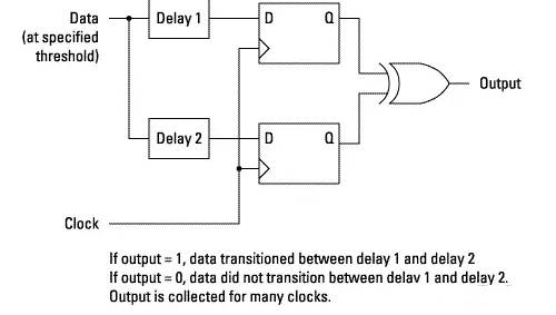 Figure 14 How Eye Positioning Works
When the unique OR output is high, the delayed samples will differ, and transitions will be detected between the delay times.
Due to the instability of the sampled signal and other variations, eye positioning measurements will check the frequency of transitions occurring between the two delay times over multiple clocks.
Then, another pair of delay values will be checked, and so on, until the entire transition time range is scanned.
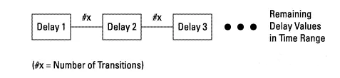 Figure 15 Recording Delay Values
Since the logic analyzer can adjust the threshold voltage of the channels, eye positioning measurements can repeatedly scan transitions over many threshold voltage levels over time.
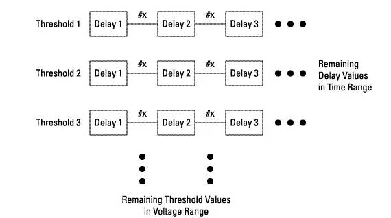 Figure 16 Multi-threshold Scanning of Eye Positioning
By adjusting the threshold voltage and viewing the activity indicators, eye positioning can find the signal activity envelope and determine the optimal threshold voltage; then by performing a full-time scan at that threshold, eye positioning can find the sample position.
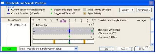 Figure 17 Scanning Thresholds and Sampling Positions in Eye Positioning
It is also possible to run a full-time scan that only automatically sets the sampling position under the current threshold voltage settings.
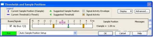 Figure 18 Only Scanning Sampling Position
Automatic threshold and sampling position setting scans are usually sufficient to ensure correct data acquisition, but they can also identify signals you want to take a closer look at (for example, if you want to check for delays, attenuation, etc.). By performing a full-time scan within the entire signal activity envelope, eye positioning can display transitions detected in small windows of time and voltage. These scans are called eye pattern scans (eye scan). Similar to an oscilloscope, eye pattern scans are used to display measurement data. The number of transitions in each window is highlighted. This can provide an overview of eye patterns and determine if further detailed examination of the signal with an oscilloscope is needed.
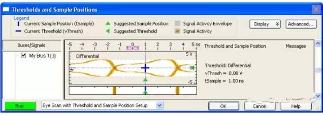 Figure 19 Eye Pattern Scan
It is possible to run an eye scan that causes automatic threshold and sampling position setting, or run an eye scan that only causes automatic sampling position setting.
Eye positioning measurements are based on the number of channels collecting data. This will affect the measurement time. When multiple logic analyzer cards exist in a module, this will be unusual; in this case, measurements will run in parallel.
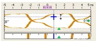
Eye Pattern Scanning in Logic Analyzers that Support Differential Signals:
Logic analyzers that support differential signals (such as the 16962A logic analyzer module) use true differential receivers for inputs:
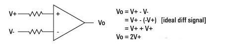
A programmable reference voltage is accounted for in the negative input. This is the threshold voltage used by the analyzer when using single-ended probes. For differential detection operations, the reference voltage is usually set to 0V:
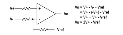
Subsequently, the output of the receiver is compared with 0V to generate internal logic signals from the differential input signal. Note that the final comparison will answer the question of whether the “differential signal is above Vref or below Vref?”
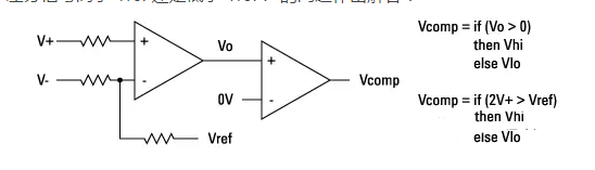
The eye gap eye scan measurement is completed through a series of eye finder measurements using different Vref settings. The default eye finder measurement for differential signals uses Vref=0V. By increasing Vref above zero, we find the position where the signal crosses the rising Vref value. If Vref rises high enough, the top edge of the signal will cross Vref, and we will see the top of the eye. Further increasing Vref will cause Vcomp to remain at Vlo, indicating that the signal will not rise to that level. Conversely, moving Vref below zero will show the bottom half of the eye.
The eye scan/eye finder display window will show the overlapping part of the eye scan graph for each signal below the eye scan graph, showing the relationship between eye finder and eye scan. By moving the Vth horizontal line up and down in the eye scan graph, the view of the eye finder at that offset from the center of the eye can be obtained.
Regardless of how the threshold is set in the user interface, the logic analyzer’s differential input will be always applied to the receiver. This means that by manually setting the voltage threshold to a non-zero value, common-mode voltage can be allowed in the differential pair. If the center of the signal swing is more than 100 mV away from the ground, eye scan will automatically perform this operation.
Triggering Logic Analyzers
Setting up the trigger of the logic analyzer is very challenging and can take a lot of time. Assuming that if you know how to program, you should be able to set the trigger of the logic analyzer effortlessly. However, this is not possible because many concepts are unique to logic analysis. The purpose of this section is to introduce these main concepts and how to use them effectively.
Conveyor Belt Analogy: We can compare the memory of the logic analyzer to a long conveyor belt, and the samples obtained from the device under test (DUT) are like boxes on the conveyor belt. New boxes are placed at one end of the conveyor belt, and fall off at the other end. In other words, due to the limited depth of the logic analyzer’s memory (the number of samples), whenever a new sample is acquired, if the memory is full, the oldest existing sample in the memory will be deleted. As shown in the figure below.
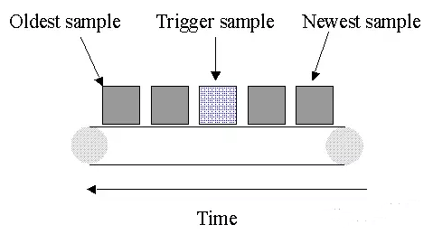 Figure 20 Conveyor Belt Analogy of Logic Analyzer Triggering
Logic analyzer triggering is like boxes placed at the starting position of the conveyor belt (which has multiple boxes on it). Their task is to “look for special boxes and stop the conveyor belt when that box reaches a specific position on the conveyor belt.” In this analogy, the special boxes are the triggers. When the logic analyzer detects a sample that matches the trigger condition, it indicates that it should stop acquiring samples when the trigger is at the appropriate position in memory.
The position of the trigger in memory is called the trigger position. Typically, the trigger position is set in the middle to maximize the number of samples that appear before and after the trigger without exceeding the memory range. However, the trigger position can also be set at any position in memory.
Due to the extensive functionality provided by logic analyzer triggering, the table below briefly summarizes the functions introduced in this article. The table will describe these functions one by one.
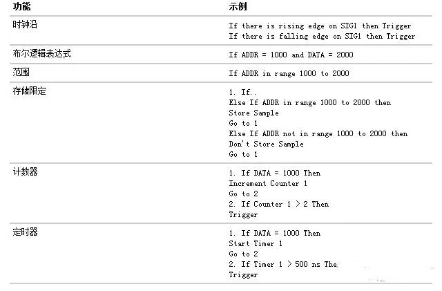 Table 1 Summary of Logic Analyzer Trigger Functions
Trigger Sequence:
Although logic analyzer triggers are usually simple, they require complex programming. For example, you might want to trigger after the rising edge of one signal followed by the rising edge of another signal. This means the logic analyzer must find the first rising edge before it starts looking for the next rising edge. Because it has a sequence of steps to look for triggers, it is called a trigger sequence. Each step in the sequence is called a sequence step.
Each sequence step consists of two parts: condition and action. The condition refers to a Boolean logic expression, such as “If ADDR = 1000” or “If there is a rising edge on SIG1”. The action refers to what the logic analyzer should execute when the condition is met. Examples of actions include triggering the logic analyzer, moving to another sequence step, and starting a timer. This is similar to an If/Then statement in programming.
Each step in the trigger sequence is assigned a number. The first step executed is always sequence step 1, but due to the “go to” action, the remaining sequence steps can be executed in any order.
When executing a sequence step and all Boolean logic expressions are false, the logic analyzer will acquire the next sample and re-execute the same sequence step. For example, consider the following trigger sequence:
1. If DATA = 7000 then TriggerIf the following samples are acquired, the logic analyzer will trigger at sample #6.
   Sample #   ADDR  DATA
   1       1000  2000
   2       1010  3000
   3       1020  4000
   4       1030  5000
   5       1040  6000
   6       1050  7000  <- Trigger position for the logic analyzer
   7       1060  2000
In reality, sequence step 1 is equivalent to “Keep acquiring more samples until DATA=7000, then trigger”.
When a sample meets the condition in a sequence step, it will always acquire another sample before executing the next sequence step. In other words, a single sample cannot meet the conditions of multiple sequence steps. Each sequence step can be seen as representing events that happen at different points in time. Two sequence steps can never be used to specify two events that occur simultaneously.
For example, consider the following trigger sequence:
    1. If ADDR = 1000 then Go to 2
    2. If DATA = 2000 then Trigger
If the following samples are acquired, the logic analyzer will trigger at sample #7.
  Sample #   ADDR  DATA
   1       1000  2000  <- This sample meets the condition in sequence step #1
   2       1010  3000
   3       1020  4000
   4       1030  5000
   5       1040  6000
   6       1050  7000
   7       1060  2000  <- Trigger position for the logic analyzer
Note that because a new sample was acquired between meeting the conditions in sequence step 1 and testing the conditions in sequence step 2, the logic analyzer will not trigger at sample #1. The trigger sequence can be seen as “Find ADDR = 1000 followed by DATA = 2000 and then trigger”. The multiple sequence steps in the trigger sequence imply “followed by”.
After the logic analyzer triggers, it will not trigger again. In other words, even if multiple samples meet the trigger condition, the logic analyzer will only trigger once. For example, using “ADDR=1000” as the trigger, if the logic analyzer acquires the following samples, it will trigger at sample #2, and only trigger at sample #2.
  Sample #  ADDR
   1       0000
   2       1000  <- Trigger position for the logic analyzer
   3       2000
   4       1000  <- The logic analyzer will not trigger again here
   5       1040
A common question is, “What happens if the condition in a sequence step is not met?” For example, if there is a condition “If ADDR = 1000 Then Trigger”, what happens if the current sample is ADDR = 2000? The logic analyzer will simply acquire the next sample and try to execute that sequence step again. In reality, if the trigger condition is “ADDR = 1000”, it is equivalent to “Keep acquiring samples until finding a sample where ADDR=1000”. Therefore, if a trigger condition is set that is never met, the logic analyzer will never trigger.
When a condition in a sequence step is met, it will be very clear which sequence step will be executed next when using the “go to” action, but if “go to” is not used, it will not be possible to know which sequence step will be executed. On some logic analyzers, if “go to” is not used, it means the next sequence step should be executed. On other logic analyzers, it means the same sequence step will be executed again. Due to this confusion, it is best to use “go to” actions rather than relying on defaults. The state and timing modules resolve this issue by automatically including a “go to” or “trigger” action in each sequence step. For example:
    If ADDR = 1000 and DATA = 2000 then
    Go to 1   <- This is automatically added
Boolean Logic Expressions: When multiple sequence steps represent “followed by”, Boolean logic expressions can be used within the sequence steps. Example:
   If ADDR = 1000 and DATA = 2000
   This expression means that ADDR must equal 1000 and DATA must equal 2000 in the same sample to meet this expression. In other words, DATA must equal 2000 at the same time ADDR equals 1000.
Therefore, if you want to trigger when two events occur simultaneously, you should use a Boolean logic expression. A common mistake is trying to use two sequence steps when a Boolean logic expression should be used, or trying to use a Boolean logic expression when two sequence steps should be used. Use Boolean logic expressions when multiple events occur simultaneously, and use multiple sequence steps when one event follows another.
Branches: Branching is similar to the Switch statement in C programming language and the Select Case statement in Basic. Branching provides a way to test multiple conditions. Each branch has its unique action. Below is an example of multiple branches:
   1. If ADDR < 1000 then Go To 2
   <- This is a branch of Level 1
      Else If ADDR > 2000 then Go To 3
   <- This is a 2nd branch of Level 1
      Else If DATA = 2000 then Trigger
   <- This is a 3rd branch of Level 1
   2. If DATA <= 7000 then Trigger
   3. If there is a Rising Edge on SIG1, then Trigger
   In sequence step 1, there are three branches, so there are three actions that can be taken.
If the condition of one branch is met, no further testing of any branches below it will occur. In other words, it is not possible to execute multiple branches based on a single sample, even if that sample could lead to the conditions of multiple branches being met. That is, each branch is an “Else If”.
Edge: An edge refers to a transition of a single signal from low to high or from high to low. Typically, edges are specified as “rising edge”, “falling edge”, or “any clock edge”, where the “rising edge” indicates a transition from low to high. On most logic analyzers, up to two edges can be included in a trigger sequence, while some only allow one edge.
Range: Specifying a range of values is a convenient way to delineate a range, such as “ADDR in the range of 1000 to 2000”. Most logic analyzers also support the “not in range” feature. A range is a convenient shortcut so you don’t have to specify “ADDR >= 1000 and ADDR <= 2000”.
Flags: A flag is a Boolean variable used to send signals from one module to another. A flag can be set when a certain condition occurs in one module and then tested later by another module. In the example below, Flag 1 is used to track what happens in the trigger sequence of Module 1, so that this information can be used in Module 2.
Module 1 Trigger Sequence:
    1. If ADDR < 5000 then
       Set Flag 1
       Trigger and fill memory
Module 2 Trigger Sequence:
    1. If DATA = 5000 and Flag 1 is set then Trigger
       Else if DATA = 1000 and not Flag 1 then Trigger
Counter: An occurrence counter is used to find the “N-th” occurrence of an event. For example, if you want to trigger when ADDR = 1000 occurs for the 5th time, you can set the trigger to:
If ADDR = 1000 occurs 5 times then TriggerA global counter is similar to an integer variable. Global counters are more flexible than occurrence counters because they can be used to count complex events (for example, an event of one clock edge followed by another clock edge). Global counters can be incremented, tested, and reset. By default, global counters start at zero and do not need to be reset unless they have been used in a trigger sequence. Generally, occurrence counters should be used over global counters when possible, as occurrence counters are simpler to use, and the number of global counters is limited.
Timer: Timers are used to check the time consumed between events. For example, if you want to trigger if another clock edge occurs within 500 ns after one clock edge appears, you would use a timer. The most critical point to remember when using timers is: start the timer first, then test it. In other words, the timer cannot be started automatically. The key to setting a timer is determining under what conditions to start and test it.
Storage Qualification: Storage qualification is used to determine whether to store (i.e., save to memory) or discard the acquired samples. This can prevent unwanted samples from occupying the logic analyzer’s memory.
Setting storage qualification is simplest by setting the “default storage”. Default storage means “store unless specified otherwise in a sequence step”. For example, if you only want to store samples when the range of ADDR is between 1000 and 2000, you should set the “default storage” to:
ADDR In Range 1000 to 2000By default, “default storage” is set to store all acquired samples. You can also set “default storage” to not store any samples, meaning that unless a sequence step overrides that default storage, no samples will be stored.
Sequence step storage qualification means only storing specific samples within a particular sequence step. This means that before leaving this sequence step using Go To or Trigger actions, this storage qualification is applied. This storage qualification is useful if you want to apply different storage qualifications for each sequence step. For example, you might not want to store any samples before ADDR = 1000, while for the rest of the measurement, only store samples where ADDR is within the range of 1000 to 2000.
Setting sequence step storage also requires using a branch instruction. For example, when looking for DATA=005E, if you only want to store samples where ADDR is within the range of 5000 to 6FFF, you can use the following sequence steps in some cases:
    1. If DATA = 005E then Trigger
       Else If ADDR in range 5000 to 6FFF then
       Store Sample
       Go to 1
    Note the use of the store sample operation. This means "immediately store the latest sample acquired in memory." It does not mean "start storing from now on." This should be noted, as when ADDR is not in the range of 5000 to 6FFF, the store sample operation is never executed, so this branch instruction essentially indicates that "only store samples where ADDR is within the range of 5000 to 6FFF in this sequence step."
The above example seems to indicate that it will only store samples where ADDR is within the range of 5000 to 6FFF. However, this depends on how the default storage is set. Using the above example, if the default storage is set to “Store Everything” and there is a sample that is not within the range of 5000 to 6FFF, the Else If branch instruction will not be executed, and the “default storage” will apply. In reality, this sequence step describes the operation to be performed when the sample value is within a specific range but does not specify what operation should be performed when the sample value is outside of that range. Therefore, to explicitly specify sequence step storage, use the following instructions:
    1. If DATA = 005E then Trigger
       Else If ADDR in range 5000 to 6FFF then
       Store Sample
       Go to 1
       Else If ADDR not in range 5000 to 6FFF then
       Don't Store Sample
       Go to 1
    Additionally, if the default storage is set to “Store Everything”, the following instructions can be used:
1. If DATA = 005E then Trigger
Else If ADDR not in range 5000 to 6FFF then
Don't Store Sample
Go to 1In summary, sequence step storage will always override default storage, but only for conditions specifically specified in sequence step storage. Caution must be exercised when handling conflicts between default storage and sequence step storage.
While setting up the logic analyzer is challenging, trigger functions can significantly reduce the difficulty of this process. Trigger functions are commonly used building blocks that can be combined to set triggers. Because these functions cover most common triggers, setting them up can be done by simply selecting the appropriate functions and filling them with data. The figure below shows the user interface for logic analyzer triggers. Note that the trigger functions are prominently located on the left side of the screen.
Figure 21 Using Trigger Functions
Generally, the biggest challenge in setting complex triggers is breaking the problem down. In other words, it is about how to map complex triggers to sequence steps, branches, and Boolean logic expressions.
-
Break the problem down into events that occur at different times. These events correspond to sequence steps.
-
Scan the list of trigger functions to try to find some that match the events identified in step 1.
-
Break down all remaining events into Boolean logic expressions and their corresponding actions. Each Boolean logic expression/action pair corresponds to a single branch in the sequence steps. Note that there may be a “store” branch that is only used to handle storage qualification for the sequence steps.
Setting up logic analyzer triggers is very different from writing software. If you can complete other tasks using pre-defined trigger functions and well-documented triggers written earlier, it can greatly reduce the difficulty of setting up logic analyzer triggers. Only when no other resources are available should you write your own trigger settings. Finally, when setting difficult triggers, break the problem down into several smaller parts and solve them one by one.
Logic Analyzer Probes
The probes of the logic analyzer are a very important part of the logic analyzer. Because logic analyzers are mainly used for online measurements, the probes provide electrical and mechanical connections to the device under test, and both aspects are major considerations when selecting probes.
As shown in the figure below, the probe passively observes the target signal, a small part of the target signal enters the probe, and is transmitted to the logic analyzer module through interconnection cables, where amplifiers in the logic analyzer module amplify this small part of the signal to restore the original waveform.
The electrical performance of the probe mainly considers two aspects, which are consistent with the considerations for oscilloscope probes.
1) Do not interfere with the target signal (signal integrity of the probe)
2) The module can accurately reproduce the measured signal (signal fidelity of the probe)
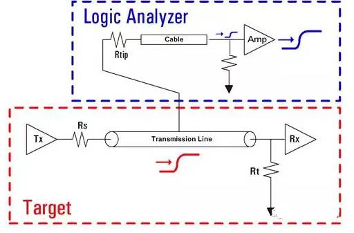
Figure 22 Probes of the Logic Analyzer
The structure of the probe is also quite complex. The small interconnection part that contacts the transmission line under test can use PCB traces, wires, connectors, or spring clips, depending on the actual situation. The front end of the probe contains resistors, which can be discrete SMT resistors or discrete resistors, generally with a resistance value of around 20k ohms. The long cable from the probe front end to the module is designed for convenience in connecting to targets at varying distances; these cables can use coaxial or twisted-pair methods, but must ensure sufficient bandwidth. The logic analyzer module needs to match the impedance of the cable to prevent signals from being reflected back, and also to amplify the incoming signals because the amplitude of the incoming signals is relatively small.
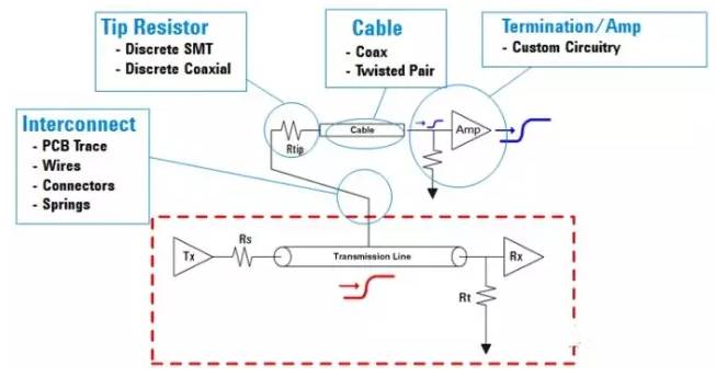
Figure 23 Considerations for Signal Integrity of Probes
The loading effects of probes can be divided into two types: DC loading and AC loading.
DC Loading: The probe appears as a DC load to ground, typically around 20K ohms. If the bus being measured has weak pull-up or pull-down characteristics (i.e., large pull-up or pull-down resistors), this load can cause logical errors. The DC load is mainly determined by the resistance of the probe tip; the larger the resistance, the smaller the DC load, and the smaller the resistance, the larger the DC load.
AC Loading: The probe contains parasitic capacitance and inductance. These parasitic parameters can reduce the probe bandwidth and cause signal reflections. We need to consider signal integrity at the receiving end of the tested circuit and at the probe tip.
The probe bandwidth is mainly reduced by two aspects: the probe capacitance and the capacitance of the cable connecting the probe to the target.
The reasons for signal reflections caused by the probe are fourfold: probe capacitance and inductance; the position where the probe is detected on the bus; the bus topology; and the length of the cable between the probe and the target.
For AC loading, we need to consider the location of the probe on the transmission line, the bus topology, and the length of the cable between the probe and the target.