Application of Embedded Logic Analyzers in FPGA Testing

Application of Embedded Logic Analyzers in FPGA Testing

Click the blue text above to follow us
The logic analyzer is an instrument that collects and displays digital signals from the test device using a clock, primarily for timing judgment. Unlike oscilloscopes, which have multiple voltage levels, logic analyzers typically display only two voltages (logic 1 and 0). After setting a reference voltage, the logic analyzer determines the measured signal using a comparator: signals above the reference voltage are considered High, while those below are considered Low, forming a digital waveform between High and Low. Similar to oscilloscopes, logic analyzers collect specified signals and present them graphically to developers, who analyze these graphical signals according to protocols to identify errors. Although graphical displays have significantly facilitated developers, manually analyzing a series of signals is cumbersome and prone to errors. In today’s rapidly advancing technological society, there is a constant pursuit of high efficiency. Automation and intelligence have become the development direction for protocol analysis. Guided by this philosophy, various testing instruments have developed protocol analysis capabilities. Currently, most developers can easily detect errors, debug hardware, and accelerate development through the protocol analysis features of testing tools like logic analyzers, ensuring high-speed and high-quality project completion. The working process of a logic analyzer involves data collection, storage, triggering, and display. Because it uses digital storage technology, it can separate data collection from display, or perform both simultaneously, and if necessary, the stored data can be displayed repeatedly for problem analysis and research.
ELA’s Working Principle and Features
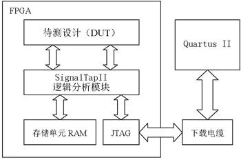
An embedded system device generally consists of an embedded computer system and an execution device. The embedded computer system comprises hardware layer, middleware layer, system software layer, and application software layer. The execution device, also known as the controlled object, can accept control commands from the embedded computer system and execute specified operations or tasks. The execution device can be simple, like a tiny motor in a mobile phone that activates when the phone is in vibration mode, or complex, like the SONY Aibo robotic dog, which integrates multiple tiny control motors and various sensors to perform complex actions and sense various state information. The block diagram of the embedded logic analyzer is shown in Figure 1, mainly divided into hardware and software parts. The hardware part consists of the design under test (DUT), the ELA IP core embedded in the FPGA, RAM storage unit, and JTAG interface; the software part includes user design software and the integrated ELA online debugging software. The working principle of ELA is: set the signals to be monitored, triggering logic, sampling depth, clock signal, and other parameters in the ELA online debugging software; compile the configured ELA file with the user design and upload it to the FPGA; run the ELA, and if the triggering conditions are met, the ELA samples the measured signal on the rising edge of the clock and stores it in the RAM storage unit.
Application of Embedded Logic Analyzers in FPGA Testing
Figure 1 Block Diagram of the Embedded Logic Analyzer
The embedded logic analyzer can conveniently perform online debugging of designs and promptly identify issues within the system without modifying the design files to obtain the status of internal nodes or I/O pins. For example, SignalTap II supports up to 1024 channels, with a sampling depth of up to 128Kb, and clock support exceeding 200MHz, with each analyzer having 10 levels of trigger input/output, thus increasing sampling accuracy.
Application of ELA in FPGA Testing
The embedded logic analyzer is widely used in FPGA testing, capable of real-time monitoring of the system. The FPGA chip used in the design is the Altera Cyclone series EP1C12Q240C8, which supports SignalTap II, has 12,060 logic elements, and a memory size of 239,616 bits, effectively supporting various complex designs.
The Application Design Process of ELA is as follows.
1. Creation of Stp File
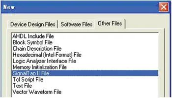
After completing and compiling the traffic light controller design, a SignalTap II file (stp file) can be created. There are typically two ways to establish an stp file: one is to directly create an stp file and configure the parameters of the logic analyzer using the SignalTap II Editor; the other is to use the MegaWizard Plug-in Manager to generate and configure the stp file, as shown in Figure 2.
Application of Embedded Logic Analyzers in FPGA Testing
Figure 2 Loading Stp File
2. ELA Settings
After adding the stp file to the design, settings can be configured as follows.
① Add Measured Signals. Use the SignalTap II Filter in Node Finder to find all signals in the design after synthesis and layout, and select the signals to be monitored. In this design, all can be selected.
② Set Sampling Clock. Any signal can be used as the sampling clock, but signals after layout cannot be used. To obtain more accurate sampling data, the global clock should be chosen as the sampling clock.
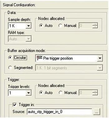
③ Determine Sampling Depth. The sampling depth of SignalTap II can reach 128Kb. When selecting sampling depth, the memory size of the FPGA must be considered; here, a sampling depth of 1Kb is chosen.
④ Set Buffer Acquisition Mode. By setting the buffer acquisition mode, the user can specify the amount of data captured before and after the SignalTap II trigger. The buffer acquisition modes mainly include circular mode and segmented buffer mode. Here, the pre-trigger position of the circular mode is selected.
⑤ Set Trigger Conditions. SignalTap II supports basic triggering and trigger functions. In basic triggering, it supports 10 levels of trigger depth, and for each trigger, different trigger levels can be set based on design needs.
The settings for SignalTap II in this design are shown in Figure 3, where the sampling depth is 1Kb, the buffer acquisition mode selects the pre-trigger position of the circular mode, and the trigger condition is basic triggering; additionally, the sampling clock is selected as the global clock. These settings can accurately perform online debugging of this design and effectively monitor internal signals.
Application of Embedded Logic Analyzers in FPGA Testing
Figure 3 SignalTap II Settings Window
3. Design
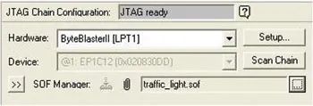
Once the stp file is set and compiled, the software embeds the ELA IP into the design, and uploads it to the FPGA. In the device list, the logic analyzer automatically detects the programmed hardware. If the FPGA chip has been selected before saving the design, it will automatically provide the selected device; if not, it needs to be selected from the device list. When the device is successfully connected, select the required SOF (SRAM Object File) in the SOF manager, and click the button to upload the design to the FPGA, as shown in Figure 4.
Application of Embedded Logic Analyzers in FPGA Testing
Figure 4 Design Window
4. Online Debugging
Online debugging involves using the JTAG interface to upload data to the debugging software, adjusting the design based on the results of real-time operation. The function achieved in this design is to determine the output for the next clock cycle (i.e., red light, green light, and yellow light) based on the current state under the control of the clock signal.
Application of Embedded Logic Analyzers in FPGA Testing
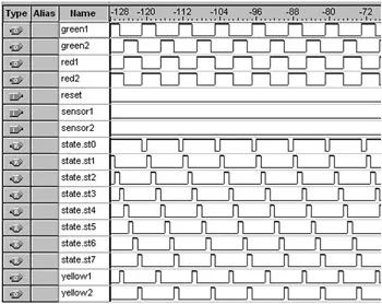
Figure 5 Real-time Monitoring Signals in SignalTap II Data Window
The waveform obtained from the design is shown in Figure 5. From Figure 5, it can be seen that for the light group, at state.st3, the yellow light is on while the green and red lights are off. After one clock cycle, it jumps to state.st4, where the yellow light is off and the red light is on; after four clock cycles, it jumps to state.st0, where the red light is off and the green light is on while the yellow light remains off; after three clock cycles, it jumps back to state.st3, where the yellow light is on and the green light is off; after one clock cycle, it jumps to state.st4, where the yellow light is off and the red light is on. The transition of the second group of traffic lights follows the same continuous cycle, thus achieving the alternating changes of the red, green, and yellow lights.
The waveform obtained during online debugging completely aligns with the required functions of the traffic light controller design. During the aforementioned debugging process, the embedded logic analyzer effectively monitored the eight internal states, ensuring the correctness of the design.
During the debugging process, users can easily start or pause the ELA to analyze internal signals. If modifications to settings, such as sampling depth or trigger conditions, are needed, simply stop the ELA, make the modifications, and recompile, thus shortening debugging time.
Application of Embedded Logic Analyzers in FPGA Testing

Scan the QR code to get

More exciting content

Application of Embedded Logic Analyzers in FPGA Testing

FPGA Design Forum

Application of Embedded Logic Analyzers in FPGA Testing

Welcome to follow ZhiXin Technology

ZhiXin Official Website: www.zxopen.com

ZhiXin Technology Forum: www.fpgaw.com

ZhiXin Technology Taobao URL:

https://zxopen.taobao.com

ZhiXin Technology FPGA Beginner Course (Bilibili):

https://space.bilibili.com/521850676

ZhiXin Technology FPGA Online Course (Tencent Classroom):

https://zxopenbj.ke.qq.com/

ZhiXin Technology – FPGA QQ Group: 282124839

For more materials download, please register http://www.fpgaw.com

Scan to add WeChat and reply to join the group

We invite you to join the FPGA study group

Application of Embedded Logic Analyzers in FPGA Testing

Welcome to join ZhiXin Technology FPGA WeChat study group. Here, you will find a group of excellent FPGA engineers, students, and teachers. The atmosphere for FPGA technology exchange and learning is strong, and everyone shares and helps each other. Bring your friends and join us!

Application of Embedded Logic Analyzers in FPGA Testing

Click to see your best

Application of Embedded Logic Analyzers in FPGA Testing

Leave a Comment