
Hello, hero! Welcome to the FPGA technology realm.This series will bring systematic learning of FPGA, starting from the basics of digital circuits, with the most detailed operation steps and the most straightforward description, providing a “fool-style” explanation, allowing students in electronics, information, communication, and newcomers to the workplace, as well as career developers looking to advance, the opportunity for systematic learning.
Systematically mastering technical development and related requirements has potential benefits for personal employment and career development; I hope it helps everyone. This time, we bring the Vivado series, the Vivado Logic Analyzer tutorial. Without further ado, let’s get started.
Vivado Logic Analyzer Tutorial
Author: Li Xirui Proofreader: Lu Hui
With traditional logic analyzers, we need to connect the signals we want to observe to the FPGA’s IO pins and then observe the signals. When there are many signals, the operation can become cumbersome. The online logic analyzer effectively solves this problem by allowing us to add these functions to the FPGA design.
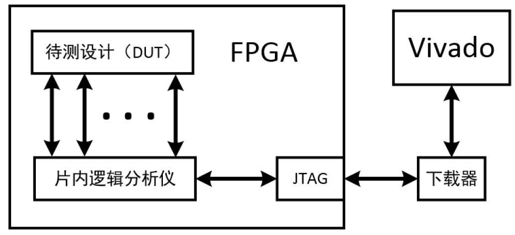
The design under test is our entire logic design module, and the online logic analyzer is also integrated into the FPGA design. It collects the signals we want to observe through one or more probes. Then, through the JTAG interface, the captured data is sent back to our user interface via the downloader for observation.
During the use of the logic analyzer, we generally have two common invocation methods:
1. IP Core
2. Mark Debug signal
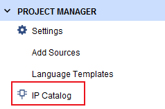
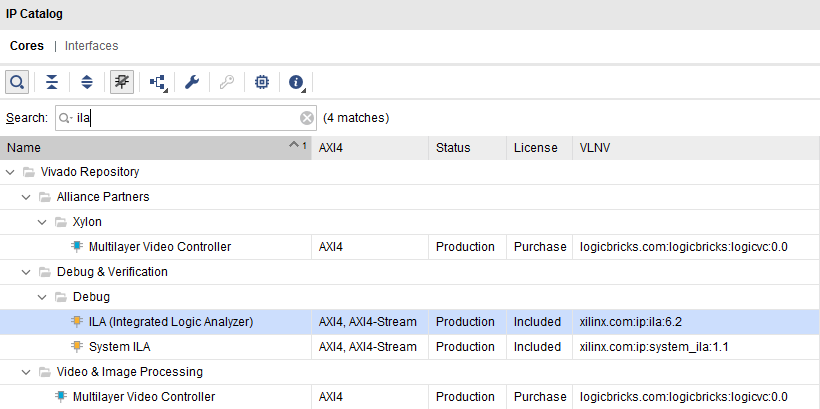
Next, let’s talk about the first method. This method requires us to open the IP core manager and instantiate the ILA in the program design. First, we open the IP core manager, search for ILA, and double-click to open it.
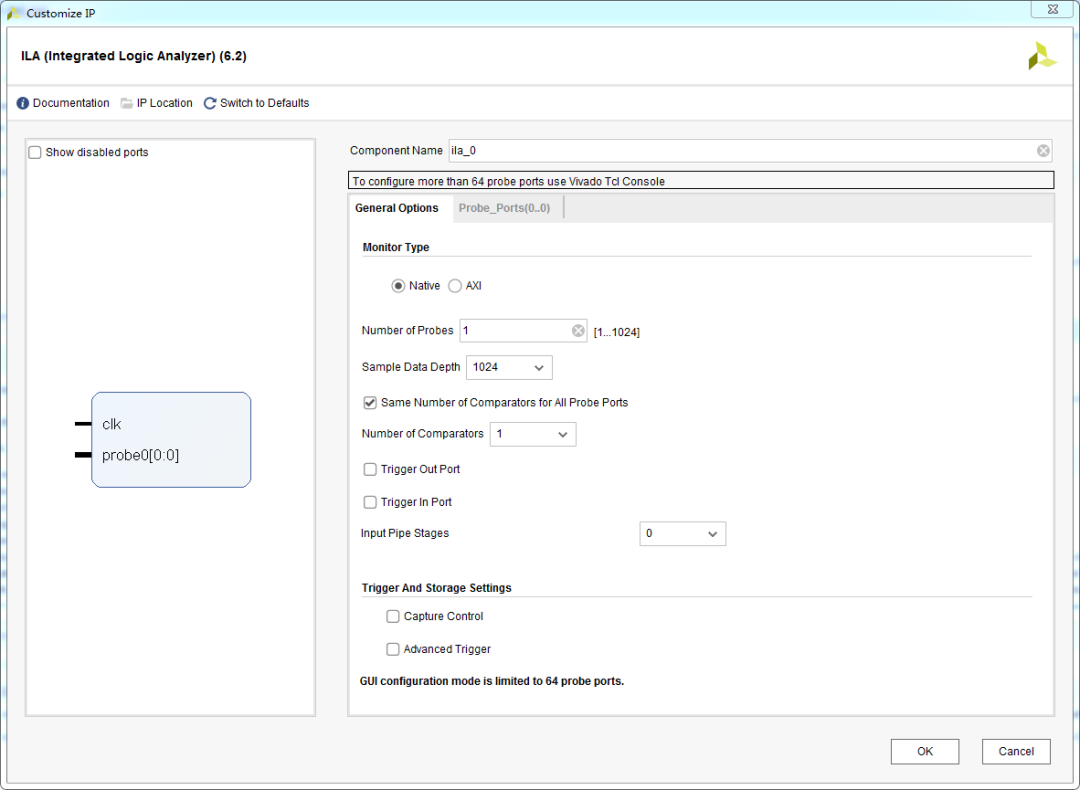
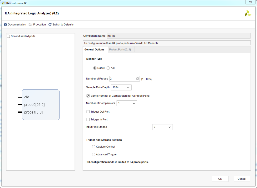
In this configuration interface, we need to configure several items. First is the Component Name, we can name our logic analyzer, for example, I will change it to my_ila.
In the number of probes option, select the number of signals we want to observe; using the example of a running light, we can observe the counter cnt in the code design and the output led. So we set this to 2. Sample data depth is the sampling depth, which affects the length of the signals we can observe; you can set it according to your needs; here I choose a depth of 1024.
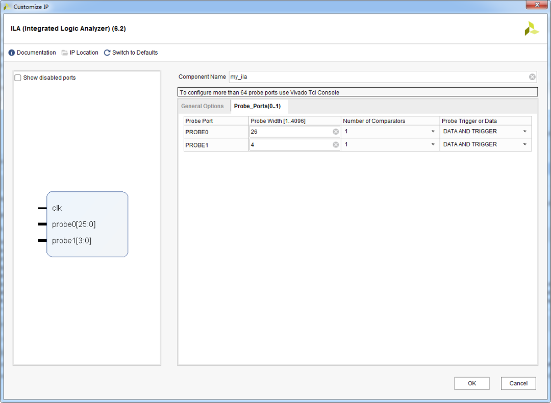
Then, set the width of the observed signal in the Probe ports. The counter is 26 bits, and the led output is 4 bits, so we set the width accordingly and click OK to generate the IP core.
Here, we briefly introduce the concept of Vivado’s Out-of-Context (OOC) synthesis. For top-level designs, Vivado uses a top-down global synthesis method, synthesizing all logic modules beneath the top level, except for modules set to OOC mode, which are synthesized independently of the top-level design. Typically, during the entire design cycle, the top-level design will be modified and synthesized multiple times. However, some sub-modules, once created, will not be modified due to changes in the top-level design, such as IPs, which are set to OOC synthesis. OOC modules are only synthesized once before the top-level synthesis. Thus, during the iteration of the top-level design, OOC modules do not need to undergo repeated synthesis, which would yield the same results. Therefore, the OOC process reduces design cycle time and eliminates design iterations, allowing everyone to save and reuse synthesis results.
Out-of-Context (OOC) synthesis is a bottom-up design process. By default, Vivado design suite uses OOC design processes to synthesize OOC modules. OOC modules can be IPs from the IP catalog, block designs from Vivado IP Integrator, or any sub-module manually set to OOC mode under the top-level module.
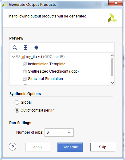
IPs from the IP catalog default to using OOC synthesis. For example, the “Synthesis Options” option in the image above is set to “Out of Context Per IP.” These IPs will be synthesized separately and generate output products (Generate Output Products), including synthesized netlists and various files before the global synthesis of the top-level. When synthesizing the top-level, OOC modules will be treated as black boxes and will not participate in the top-level synthesis. After the synthesis, during the implementation process, the black boxes of OOC modules will be opened, and their netlists will be visible and participate in the global design’s layout and routing.
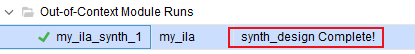
After OOC synthesis, it looks like this:
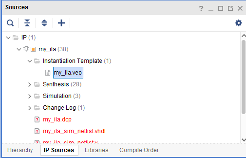
After completing the IP core invocation, we open the instantiation template of the IP core in the IP sources window. Taking the my_ila.veo file as an example, we double-click to open it and copy the content into the top-level file.
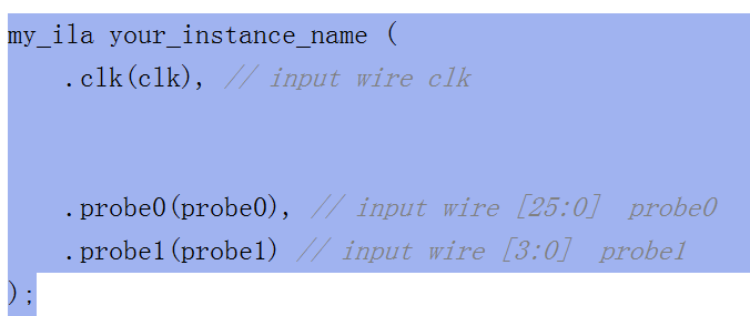
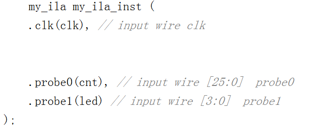
After copying, we will connect the signals and change the instantiation name. Thus, our logic analyzer invocation is complete.
After invocation is complete, we save the file and generate the board file for downloading.
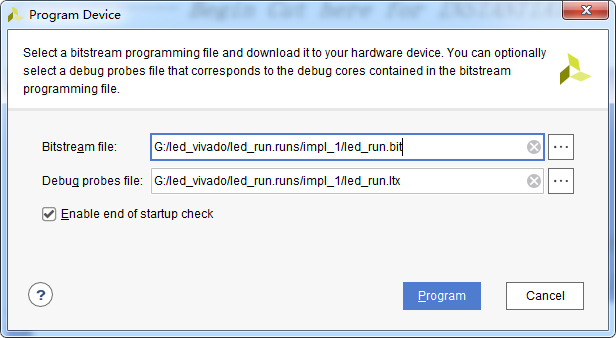
During downloading, two files appear in the interface. The first file is the bitstream file. The second is the logic analyzer file. Just click program. After downloading, the following interface will appear.
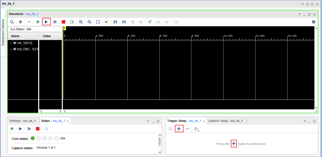
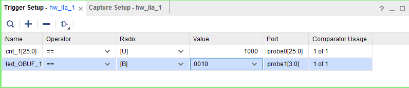
Before we start observing the waveforms, we need to set the trigger signal in the small window at the bottom right. This can be understood as the position of the waveform we want to observe. For example, we can observe the second light of the led being on and the counter reaching 1000, so our settings are as follows:
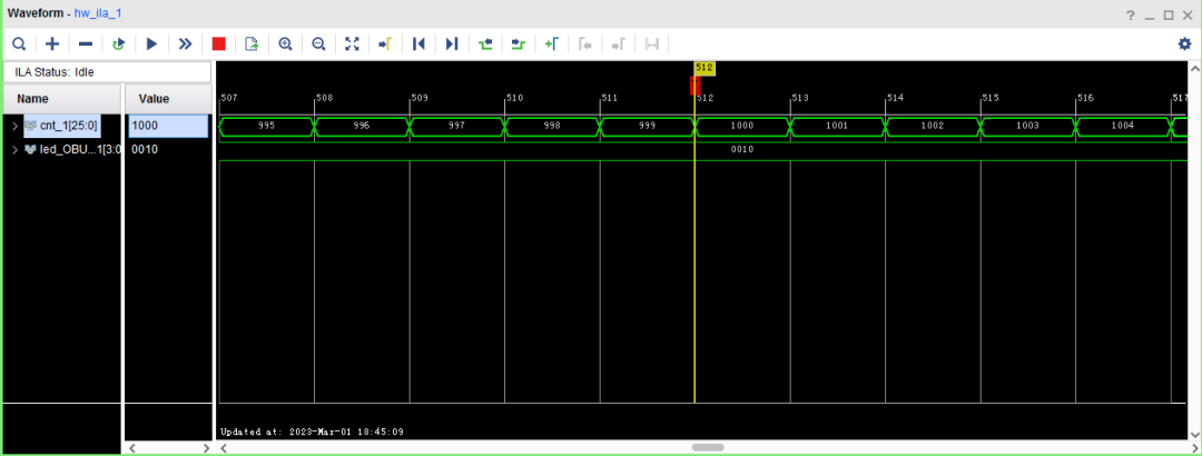
Once set, we click the triangular symbol on the waveform interface to trigger, and we can observe our waveform.
Second method:
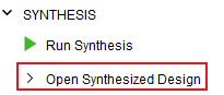
The “Netlist Insertion Debug Probe Process” requires marking each signal to be debugged within the synthesized netlist with the “Mark_Debug” attribute, and then using the “Setup Debug” wizard to set the parameters of the ILA IP core. Finally, the tool will automatically create the ILA IP core based on the parameters. We click the “Open Synthesized Design” button in the “Flow Navigator” window as shown below:
In the window layout selector of the synthesized design, we select the “Debug” window layout as shown below:
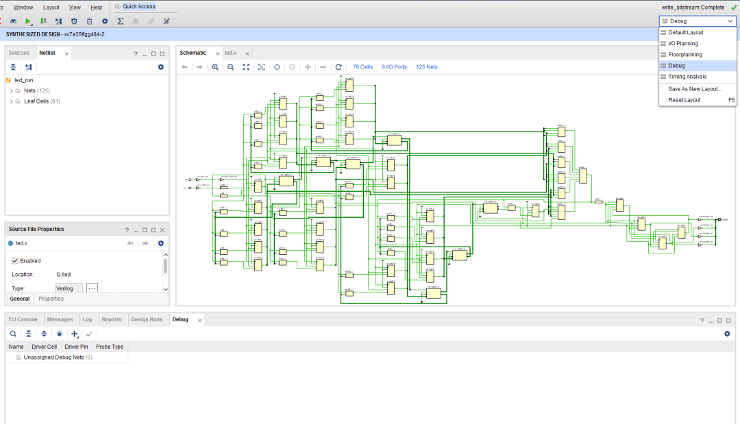
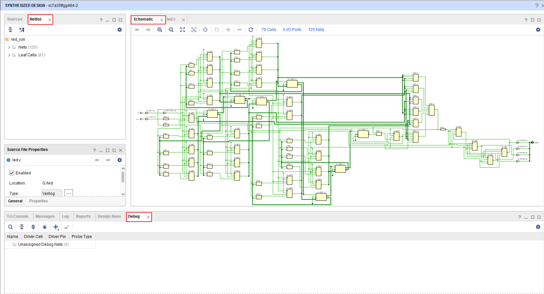
At this point, Vivado opens the “Netlist” sub-window, “Schematic” sub-window, and “Debug” sub-window. The “Netlist” and “Schematic” sub-windows are used to mark the signals to be observed, while the “Debug” sub-window displays and sets the parameters of the ILA IP core. As shown below:
In the “Debug” sub-window, there are two tabs: “Debug Cores” and “Debug Nets.” Both tabs are used to display all signals marked as “Mark_Debug.” The difference is that the “Debug Cores” tab provides a view centered around the ILA IP core, showing all signals marked as “Mark_Debug” that have been assigned to ILA probes under the respective ILA IP core view tree, while signals marked as “Mark_Debug” but not yet assigned to ILA probes are displayed under “Unassigned Debug Nets.” You can also view and set various properties and parameters of the ILA IP core in this tab. The “Debug Nets” tab only shows signals marked as “Mark_Debug” but does not display the ILA IP core; all signals marked as “Mark_Debug” that have been assigned to ILA probes will be displayed under “Assigned Debug Nets,” while signals marked as “Mark_Debug” but not yet assigned to ILA probes are displayed under “Unassigned Debug Nets.”
First, we mark the signals to be observed. Taking the led signal as an example, find the “led_OBUF” network under the “Nets” directory in the “Netlist” sub-window, right-click that network (at this point, the “Schematic” sub-window on the right will also automatically highlight this network since the objects in the “Netlist” and “Schematic” sub-windows are cross-selected), and select the “Mark Debug” command from the pop-up menu as shown below:
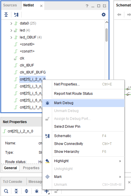
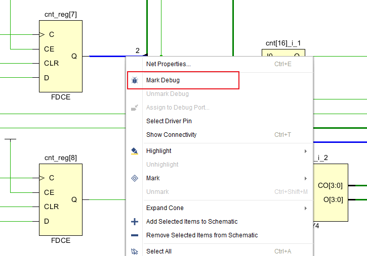
You can also select the network in the “Schematic” sub-window and then right-click to choose the “Mark Debug” command as shown below:
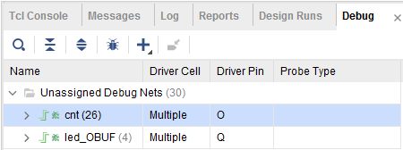
Additionally, you can add the “Mark Debug” attribute to the reg or wire signals you want to observe in the HDL source code, for example: (* mark_debug = “true” *)reg [25:0] cnt; where “(* mark_debug = “true” *)” must be placed immediately before the variable declaration. After synthesis, when you open the synthesized design, the counter signal will be automatically marked with the “Mark Debug” attribute. At this point, in the “Debug” sub-window under the “Debug Nets” tab, the “Unassigned Debug Nets” directory will show the signals we just marked, “led_OBUF.”
At this point, the “Debug” sub-window’s “Debug Nets” tab’s “Unassigned Debug Nets” directory contains the signals “led_OBUF” and “cnt” as shown below:
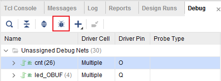
Next, we click the “Setup Debug” button in the “Debug” sub-window as shown below:
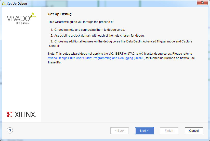
The “Setup Debug” wizard will pop up, and we directly click next as shown below:
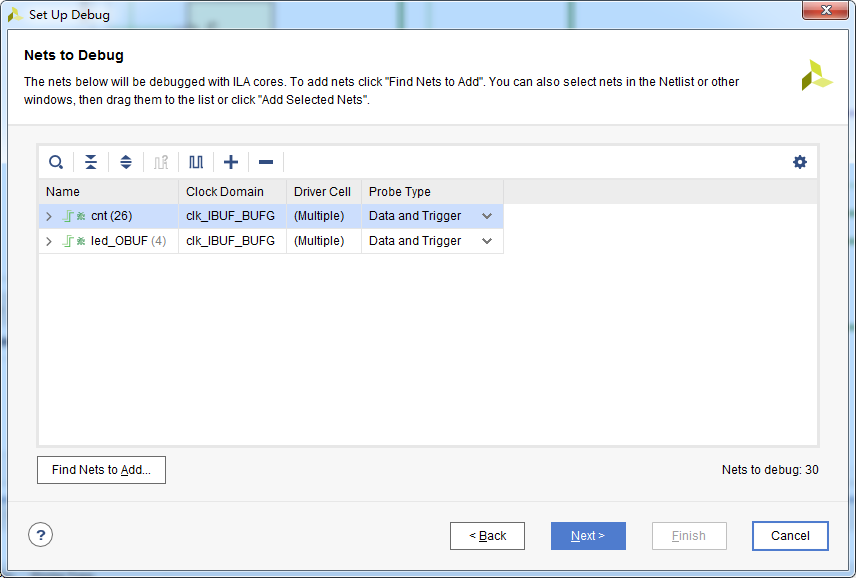
The next page is to select the clock domain used for sampling the signals to be tested. Vivado will automatically recognize the clock domains of the signals to be tested and set them as their sampling clocks. For example, the two signals we just added, “led_OBUF” and “cnt,” belong to the “sys_clk_IBUF” clock domain, and Vivado has automatically set “sys_clk_IBUF” as the sampling clock for these two signals as shown below:
Of course, users can also manually specify the clock domains for sampling the signals to be tested by right-clicking the signals to be tested and selecting “Select Clock Domain,” which will pop up the “Select Clock Domain” window as shown in the following two images:
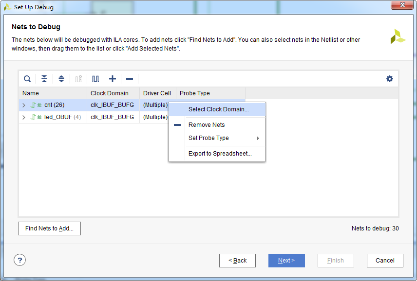
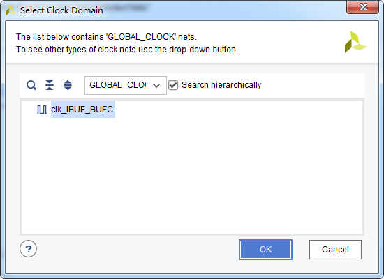
In the “Select Clock Domain” window, you can choose the clock to be used for sampling the signals to be tested. The “Setup Debug” wizard will generate a separate ILA IP core for each sampling clock. Since there is only one clock in this example, only one ILA IP core will be generated here. After setting the sampling clock, we click next, and the next page is used to set the global settings of the ILA IP core as shown below:
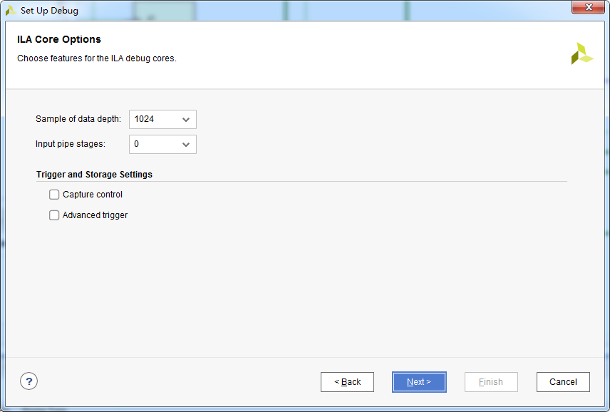
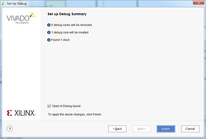
Among them, “Sample of data depth” is used to set the sampling depth, and “Input pipe stages” is used to set the synchronization stages between the signals to be tested and their sampling clocks. If there are asynchronous signals to be tested in the previous clock domain setting page, this value should not be less than 2 to avoid metastability. Since the two signals to be tested in this example are synchronized with their sampling clocks, this can be set to 0. We click next to go to the final overview page, and after confirming that everything is correct, we directly click finish as shown below:
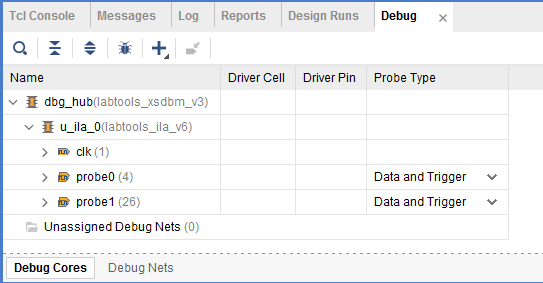
In the “Debug” sub-window under the “Debug Cores” tab, you can see that Vivado has added the ILA IP core, and there are no unassigned signals in the “Unassigned Debug Nets” directory as shown below:
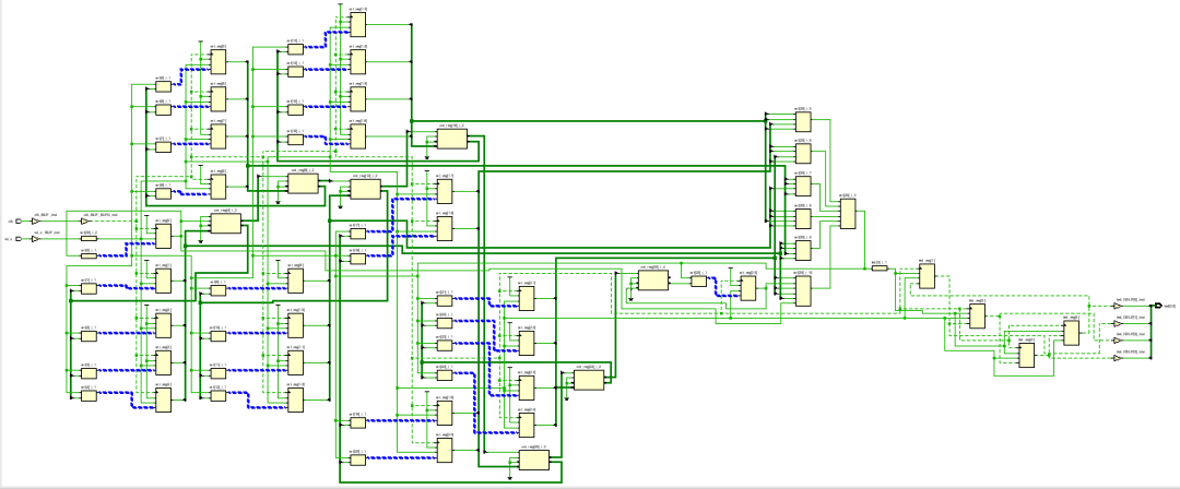
The signals in the netlist marked as Mark Debug have also turned into dashed lines to indicate that they have been allocated to the ILA IP core as shown below:
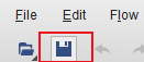
As mentioned earlier, in the “Netlist Insertion Debug Probe Process,” the debugging information set by the user will be saved in the form of Tcl XDC debug commands in the XDC constraint file. During the implementation phase, Vivado will read these XDC debug commands and include these ILA IP cores during layout and routing. At this point, all changes and settings we made are still only in the computer’s memory; we need to save them in the hard disk’s XDC constraint file by clicking the save button in the toolbar as shown below:
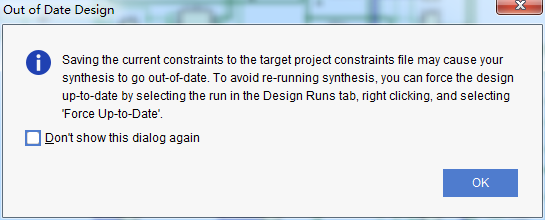
In the dialog box that appears, click OK directly as shown below:
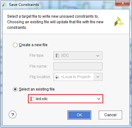
The popped-up “Save Constraints” window asks the user which XDC constraint file to save the constraints in. In this example’s project, there is only one XDC constraint file as shown below; we can click OK directly:
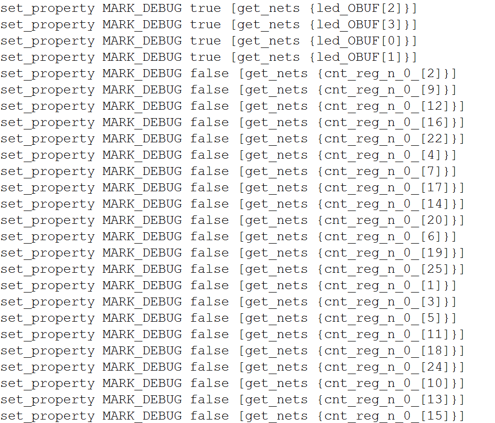
At this point, if we open led_twinkle.xdc, we will see that under the user constraints, Vivado automatically writes the debug constraints as shown below:
During the implementation phase, Vivado will read these constraints and automatically include the ILA IP cores during layout and routing according to the parameters of these commands. Thus, we have successfully added the ILA IP core to the design using the “Netlist Insertion Debug Probe Process.” Next, we can implement the design and generate the bitstream, and finally download the bitstream to the FPGA for online signal observation. This part has already been introduced in the first method above, so it will not be repeated.

– End –


FPGA Technology Realm is Broadly Inviting Heroes
Ad-free pure mode, providing a clean space for technical exchanges, from beginners to industry elites and industry leaders, covering various directions from military to civilian enterprises, from communication, image processing to artificial intelligence, there is something for everyone. QQ and WeChat dual selection, FPGA technology realm creates the purest and most professional technical exchange learning platform.
FPGA Technology Realm WeChat Group

Add the group owner’s WeChat, noting your name + company/school + position/major to join the group
FPGA Technology Realm QQ Group

Please note your name + company/school + position/major to join the group