
This series will provide a systematic study of FPGA, starting from the basics of digital circuits, with the most detailed operational steps and straightforward descriptions. It aims to offer a hands-on, “foolproof” explanation that allows students in electronics, information, and communications, as well as new professionals and developers looking to advance their careers, to have a systematic learning opportunity.
Systematically mastering technical development and related requirements can potentially aid personal employment and career development. We hope this will be helpful for everyone. In the future, we will gradually update the content related to the development of Xilinx’s Vivado, ISE, and other related software. Learning FPGA design methods and ideas in conjunction with practical software operations will make your journey in technical learning smooth, allowing you to bid farewell to small technical bugs and misleading training inducements, and truly learn and apply your skills. Without further ado, let’s get started.
Signal Tap Logic Analyzer Tutorial
Author: Xu Shuai Hao Proofreader: Lu Hui
In previous design developments, we used ModelSim to obtain data from a certain unit, and the inputs were provided by the designer in the testbench. However, in practical applications, the external input signals may not match those described in the testbench, which can lead to successful RTL simulation but failed board testing.
The Signal Tap Logic Analyzer captures and displays real-time signal behavior in FPGA designs, allowing us to inspect the behavior of internal signals during normal device operation without additional I/O pins or external laboratory equipment.
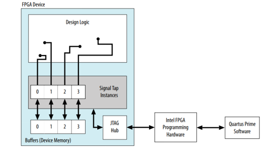
During data acquisition, the memory module in the device stores the collected data, which is then transmitted to the logic analyzer via the JTAG communication cable.
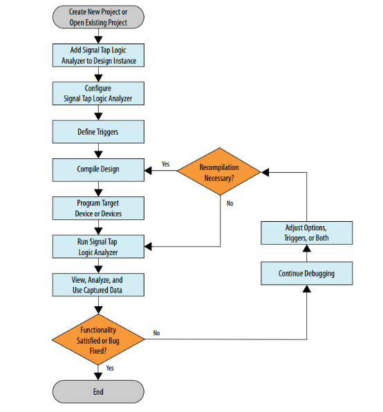
The following diagram illustrates the task flow of the Signal Tap Logic Analyzer.
-
Design Requirements
Use the logic analyzer to measure the bit time width of UART (at a baud rate of 115200) sent from the computer.
-
Design Analysis
In the UART protocol, the time width of each bit is specified as 1 second divided by the baud rate. However, in practical circuits, two oscillators with the same label may have some error. We can use the logic analyzer (specifically, the FPGA’s clock) to measure the bit time width when the PC sends UART data.
Since the baud rate is 115200, a 16x oversampling is generally used during sampling. At this point, the sampling frequency is relatively high, and the basic 50MHz clock cannot provide an accurate 16x oversample, which may introduce some error.
Using the logic analyzer, we can observe the real sampling deviation under these two conditions and determine whether the deviation affects our design.
-
Design Implementation
Copy the _9_uart_drive and rename it to _10_uart_drive_signal_tap. Then open this project and change the baud rate to 115200.
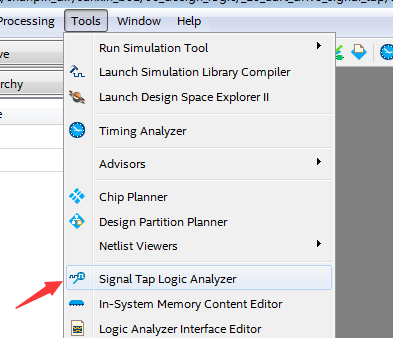
Click on tools -> Signal Tap Logic Analyzer.
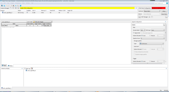
In the right window of the signal configuration, you first need to specify a sampling clock signal.
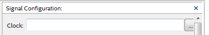
The logic analyzer samples data on each rising edge of the sampling clock. The logic analyzer does not support sampling on the falling edge of the sampling clock. Any signal in the design can be used as the sampling clock. However, to achieve the best data sampling results, use a global clock synchronized with the signal being measured.
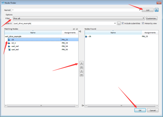
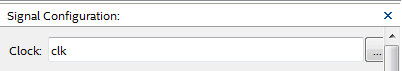
In this design, all signals are driven by an external clk signal, so we select clk as the sampling clock. Click the three dots next to the clock dialog box. Set the filter to pin: all, click list, select clk in matching nodes, click ‘greater than’, and clk will appear in nodes found, then click ok.
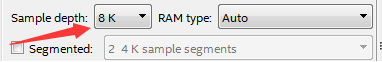
After configuring the sampling clock signal, you need to configure the sampling depth.
For each signal in the sampled data, the sampling depth specifies the number of samples to be taken and stored. In cases where device memory resources are limited, if the selected depth is too large, the design may fail to compile. In this case, you need to reduce the sampling depth to decrease resource usage.
The sampling depth multiplied by the sampling interval determines the sampling time width. Now we want to sample a UART protocol frame, which consists of 12 bits. At a baud rate of 115200, the sampling time width should be 104166ns, so the sampling depth should be 5208. Therefore, we select a sampling depth of 8K.
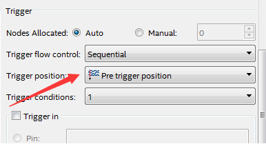
Once the sampling depth is determined, you can specify the amount of data to be sampled before and after the trigger event.
The logic analyzer offers three options. Pre indicates that 12% of the storage depth is used for data before the trigger event, and 88% for data after; Center indicates 50% for data before and 50% for data after; Post indicates 88% for data before and 12% for data after.
We select Pre here.
After configuring this information, start adding the signals you want to observe.
In the setup interface, double-click on the blank area to add the signals you want to observe.
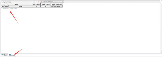
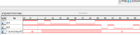
The signals to be observed are uart_txd, uart_rxd, and cap_cnt.
uart_txd and uart_rxd are port signals, so when selecting the filter, choose PIN: all. cap_cnt is an internal signal, so when selecting the filter, choose signal tap: pre-synthesis.

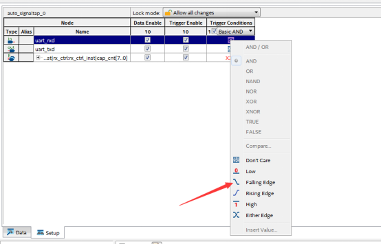
Set the falling edge of uart_rxd as the trigger condition.
Right-click on the trigger conditions of uart_rxd and select falling edge.
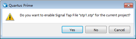
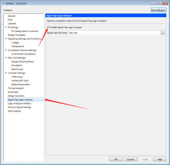
Click save to save it to qprj, naming it stp1.stp.
Enable the logic analyzer. Click Yes.
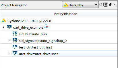
Return to the Quartus interface, perform synthesis analysis, and generate the configuration file.
In the project wizard’s structure interface, you can see two unknown components appear in the structure. These are the logic analyzers.
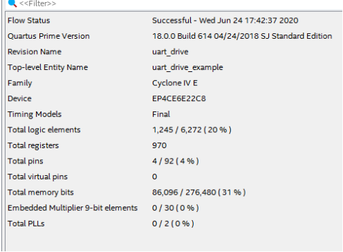
The report shows that the used logic and memory resources have increased.
Return to the signal tap interface and connect the PC and the development board.
Select USB – blaster in hardware.
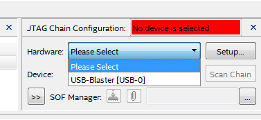
Click the three dots next to the sof manager, select the generated sof file, and then click download.
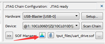
Click run analysis.
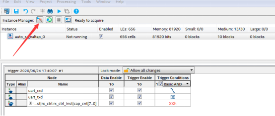
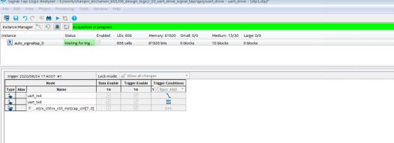
At this point, the logic analyzer is waiting to be triggered.
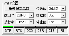
The trigger condition is the falling edge of uart_rxd. Open the serial assistant, configure it, and send data 11.
After sending, the waveform appears in the logic analyzer. Since the data sent is 11, the first data should be 1, starting with a low level. Thus, the first low level indicates the start bit, and we can determine its time width through the sampled digital number.
Left-click to zoom in, right-click to zoom out.
The left side is 0 because we used the falling edge as the trigger condition. Zooming in on the left side shows the number 434.
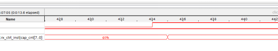
Therefore, the time width of the start bit is 434x20ns, which equals 8680ns. According to the baud rate of 115200, the time width of each bit should be 8680.5556ns. This confirms that the bit time width sent from the PC matches our expectations.
This method can be used to measure the width of other bits; some bits may be shorter than 8680ns, while others may be longer, but the deviation is generally small.
Since the actual width differs from our expected width, it is important to note that the design assumes each bit width is an integer multiple of 20ns, which can introduce deviation during sampling. This can be observed through cap_cnt, and as the sampling length increases, the accumulated error will also increase.
At the first bit of the data, cap_cnt equals 7, and it should change to 8 soon. According to the counting rule of cap_cnt, it is designed for 16x oversampling, so all subsequent bit starts should be 16*N + 7 and then quickly change to 16*N + 8. However, the actual time width shows some deviation from the expected time width.
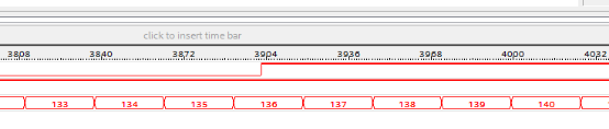
At the start of the last parity bit, according to the 16x oversampling of cap_cnt, it should be 135, then quickly change to 136. However, it is already equal to 136 and is about to change to 137.
We sample based on cap_cnt (sampling at the positions where cap_cnt changes).
Due to the errors, it is stipulated that the UART protocol frame length should not be too long, meaning the number of data bits in between cannot be arbitrarily increased.
The numerical results of the above analysis are the author’s test results, and different PCs and development boards may yield different results during testing.
-
Logic Analyzer Summary
Using the logic analyzer allows us to directly observe the waveforms running inside the development board. Therefore, it is often used for board-level testing as the final result.
If the logic analyzer is not needed in the project, you can open assignments -> settings -> signal tap logic analyzer, uncheck the enable box, and then recompile.

Selected Previous Issues


[Free] FPGA Engineer Recruitment Platform
FPGA talent recruitment, HR from enterprises, look here!
Selected System Design | Real-Time Image Edge Detection System Design Based on FPGA (with Code)
Design of Gigabit Ethernet RGMII Interface Based on Primitives
Timing Analysis Theory and TimeQuest Usage_Chinese Electronic Version


FPGA Technology Community Invites You
No ads, pure mode, providing a clean space for technical exchanges. From beginners to industry elites and leaders, from military to civilian enterprises, covering all directions from communication, image processing to artificial intelligence, QQ and WeChat dual selection, the FPGA technology community builds the purest and most professional technical exchange learning platform.
FPGA Technology Community WeChat Group

Add the group owner’s WeChat, note your name + school/company + major/job to join the group
FPGA Technology Community QQ Group

Note: Name + School/Company + Major/Job to join the group