From the intense computing power competition of AI large models to the “chip” battle in new energy vehicles, and to every smart device around us, a powerful “Chinese chip” is pulsating behind it. This is no longer distant technology news, but a global wave of a “new gold rush” that concerns the future.
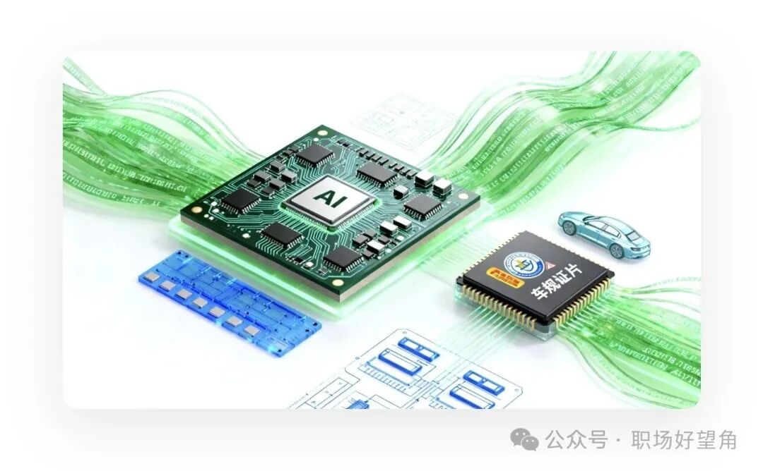
Since 2023, the semiconductor industry has welcomed a dual dividend of “policy + market”, accelerating domestic substitution and technological iteration, becoming a hot track pursued by global capital and talent. Whether professionals want to cross over to share the pie, job seekers want to enter precisely, or entrepreneurs want to find the right wind, this comprehensive guide covering segmented fields, company distribution, and job opportunities is worth your collection and sharing!
1. Five Key Segments of the Semiconductor Industry: Technical Barriers + Development Trends, Understanding the Core Logic of the Industry
The semiconductor industry chain is interconnected, from design to manufacturing to equipment materials, each segment has its unique technical barriers and growth potential. Beginners should first understand these five major sectors and the panoramic view:
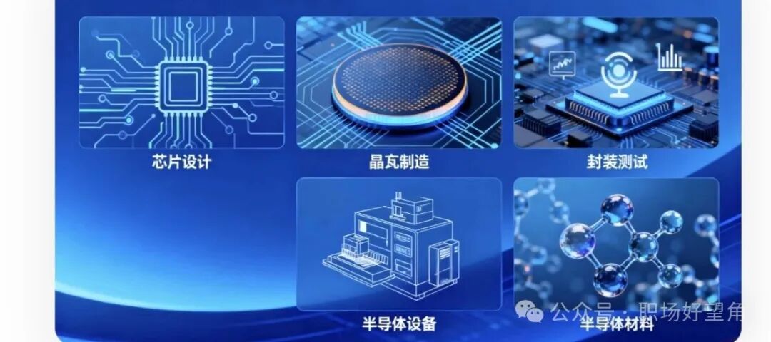
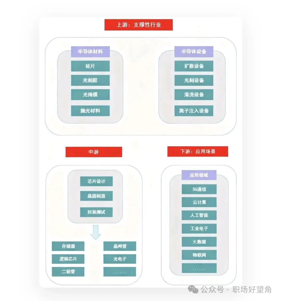
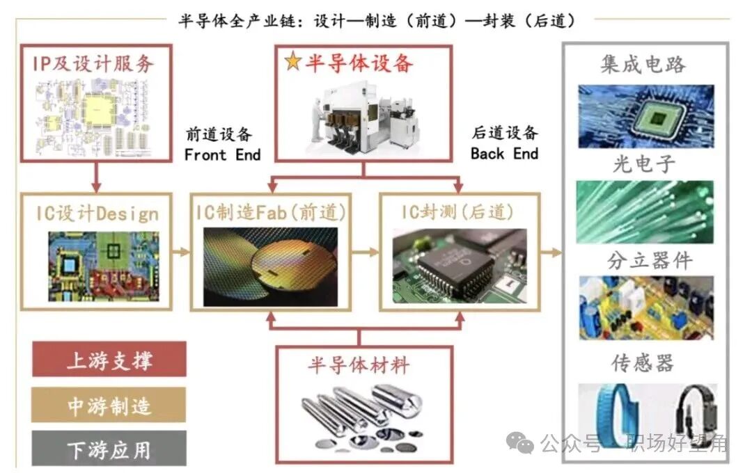
1. Chip Design: The “Brain” of the Industry, AI + Automotive Standards as Growth Engines
As the core link of the semiconductor industry chain, chip design is responsible for defining chip functions and architecture, directly determining product performance. Currently, the global market is dominated by giants like NVIDIA and Qualcomm, but domestic companies are accelerating their breakthroughs.
– Development Dynamics: AI chips are experiencing explosive demand due to the computing power needs of large models, with NVIDIA occupying the high-end market thanks to its CUDA ecosystem; automotive chips are seeing a surge in demand due to the increasing penetration of autonomous driving, with domestic companies like Chipone Technology achieving gross margins over 30%, but automotive certification cycles can take 2-3 years.
– Future Trends: There is vast potential for domestic substitution, with AI chips, automotive chips, and industrial control chips becoming key breakthrough areas. Companies with independent architectures will be more competitive.
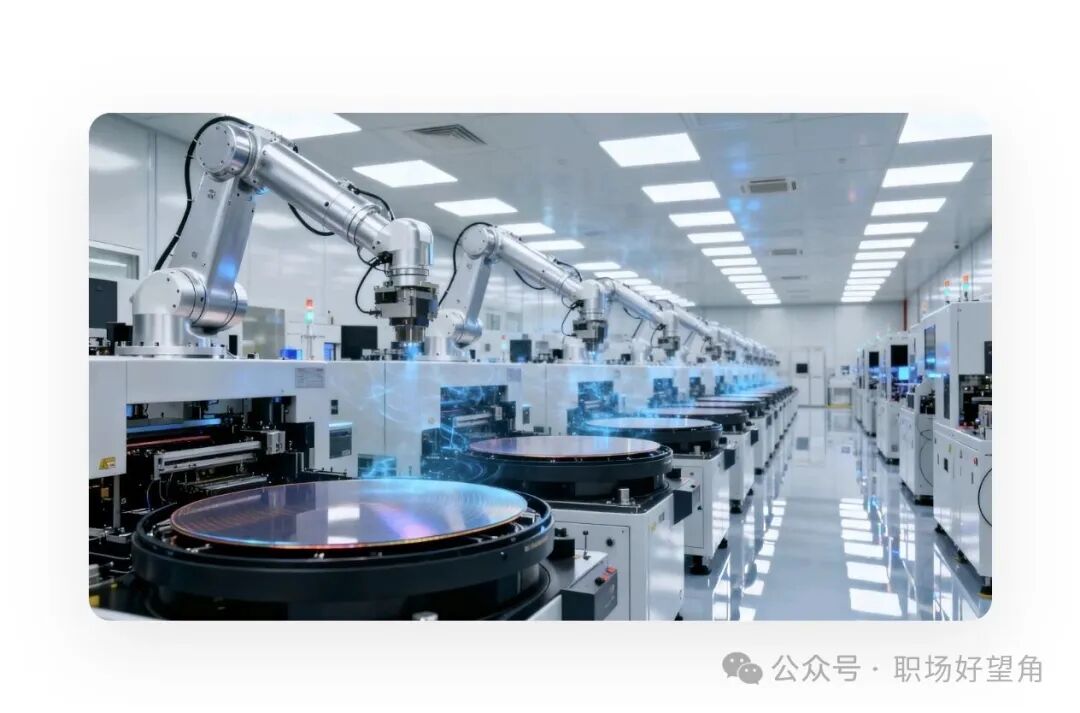
2. Wafer Manufacturing: The “Core Workshop” of the Industry, Expanding Mature Processes + Breaking Through Advanced Processes
Wafer manufacturing is the key step in converting design blueprints into physical chips, with the highest technical complexity and capital investment.
– Development Dynamics: SMIC has achieved mass production of 14nm FinFET technology, and Hua Hong Semiconductor’s 90nm BCD process is globally leading, mainly applied in power devices; due to geopolitical influences, imports of advanced process equipment below 14nm are restricted, but mature processes (28nm and above) are continuously expanding due to demand from automotive and IoT sectors.
– Future Trends: “Mature process expansion + advanced process breakthroughs” will run in parallel, with domestic wafer factories investing over a trillion yuan, and demand for equipment and materials will continue to explode.
3. Packaging and Testing: The “Packaging and Quality Control” of Chips, Advanced Packaging as a Technical Breakthrough Point
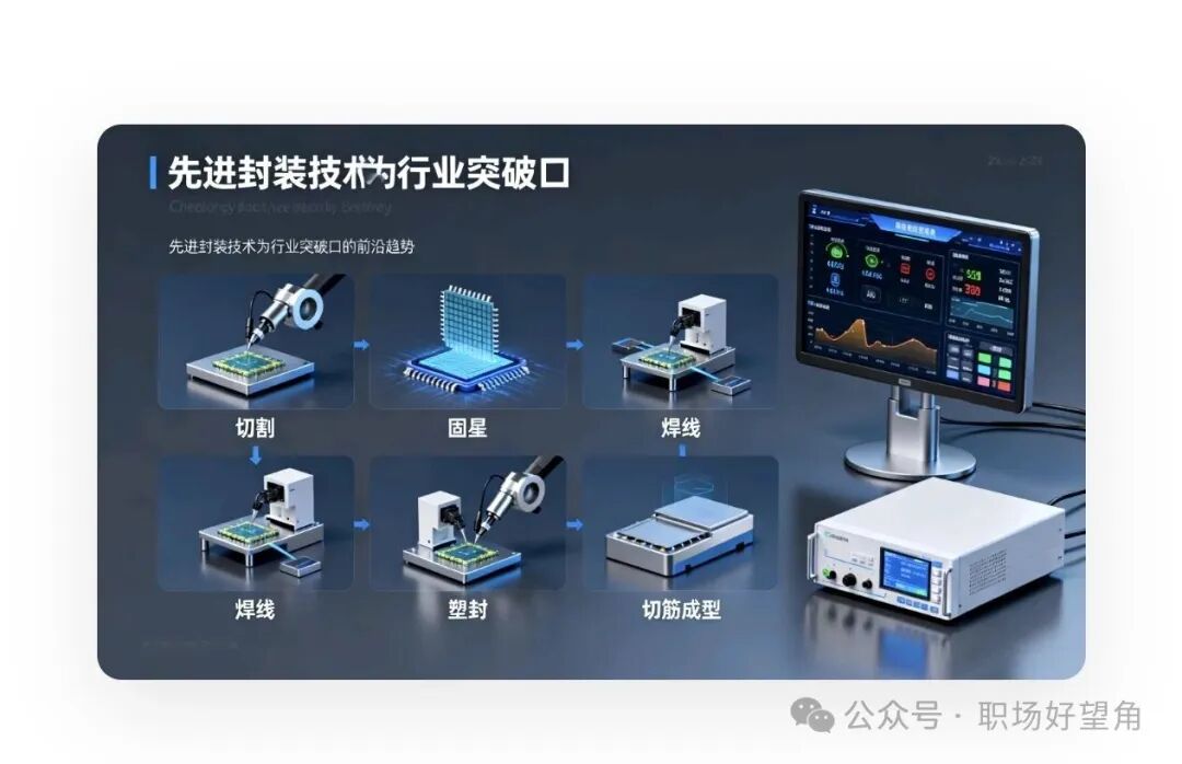
Packaging and testing are responsible for the packaging, cutting, and performance testing of chips, representing the “last mile” of the semiconductor industry chain. The technical barriers are relatively low, but advanced packaging has become the focus of differentiated competition.
– Development Dynamics: JCET’s 4nm Chiplet packaging technology has reached an internationally leading level, and Tongfu Microelectronics has become a core packaging and testing partner for AMD; AI chips and high-end processors are driving a growth in demand for 2.5D/3D packaging, with a market growth rate exceeding 20% annually.
– Future Trends: Packaging technology is upgrading towards high density and high integration, with Chiplet technology becoming a standard for advanced chips. Domestic companies are expected to achieve “curve overtaking” in the advanced packaging field.
4. Semiconductor Equipment: The “Foundation of the Industry”, Urgent Need to Improve Domestic Production Rate
Semiconductor equipment is the core support for wafer manufacturing and packaging testing, including etching machines, thin film equipment, photolithography equipment, etc., directly determining the precision and yield of chip manufacturing.
– Development Dynamics: Shanghai Micro Electronics Equipment has entered TSMC’s supply chain with its 5nm etching machine, and North Huachuang’s plasma etching machines and thin film deposition equipment cover multiple core links; currently, the domestic self-sufficiency rate of semiconductor equipment is less than 20%, with policies clearly requiring a self-sufficiency rate of 70% by 2025.
– Future Trends: As domestic wafer factories expand, equipment demand will continue to grow, with strong policy support, and the domestic production rate will steadily increase, ushering in a “golden development period” for equipment companies.
5. Semiconductor Materials: The “Raw Materials” for Chips, Breakthroughs in High-End Fields Imminent
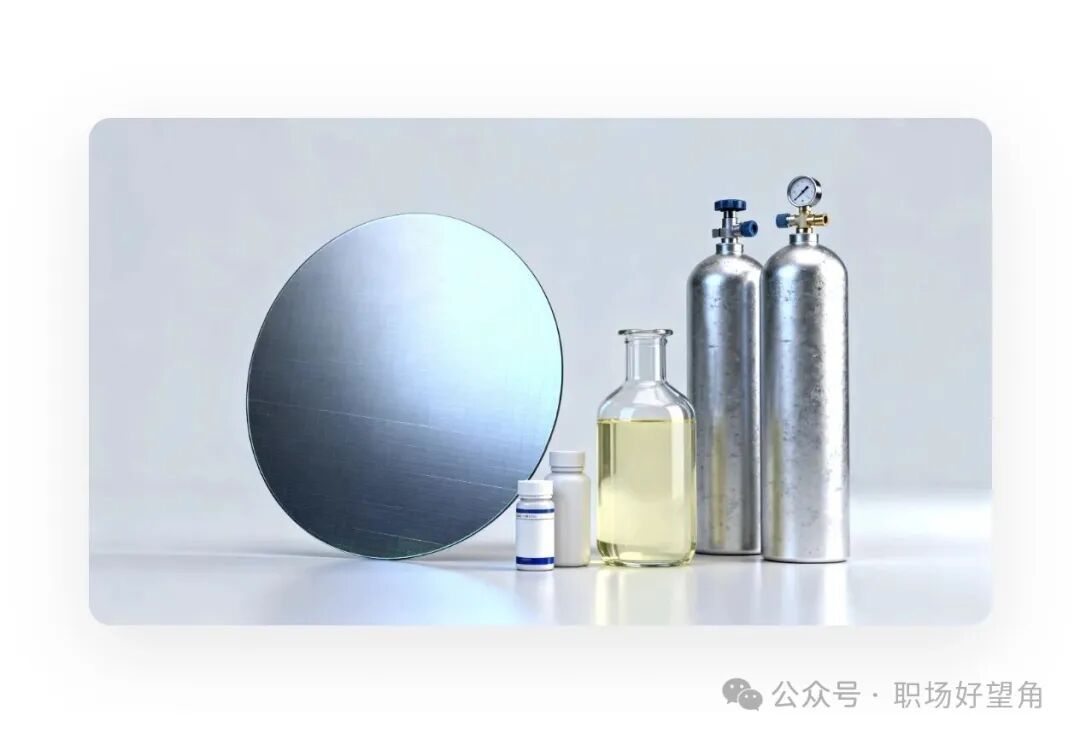
Semiconductor materials include large silicon wafers, photoresists, specialty gases, etc., which are the foundation of semiconductor manufacturing and directly affect chip performance and cost.
– Development Dynamics: Shanghai Silicon Industry’s 300mm large silicon wafer yield exceeds 90%, achieving import substitution; Nanda Optoelectronics’ ArF photoresist has been validated by SMIC, breaking foreign monopolies; high-end materials have long relied on imports, but domestic companies are gradually breaking through technical barriers.
– Future Trends: Materials are advancing towards high-end and self-sufficiency, with 300mm large silicon wafers, ArF/KrF photoresists, and high-purity specialty gases becoming key breakthrough areas, with vast market potential.
2. Map of Major Semiconductor Companies: Four Major Industrial Zones + Core Companies, Identifying Employment Destinations
The semiconductor industry shows a clear regional clustering effect, with three core industrial zones formed in China: the Yangtze River Delta, Beijing-Tianjin-Hebei, and the Pearl River Delta, as well as emerging industrial clusters in Hefei, Chengdu, and Xi’an, with company distribution highly matched to regional advantages:
1. Yangtze River Delta: The Core Gathering Area of the Industry (over 50% share)
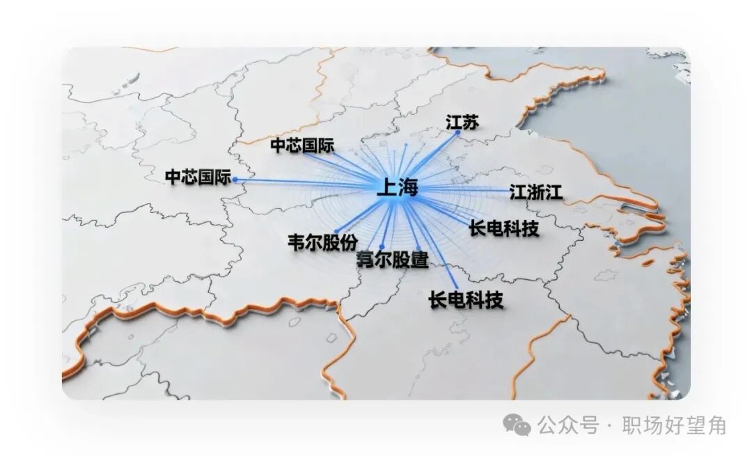
– Shanghai: SMIC (wafer manufacturing), Weir Shares (chip design), Shanghai Silicon Industry (semiconductor materials), Shanghai Semei (semiconductor equipment)
– Jiangsu: CR Micro (wafer manufacturing), Tongfu Microelectronics (packaging testing), JCET (packaging testing)
– Zhejiang: Silan Microelectronics (wafer manufacturing), Jiangfeng Electronics (semiconductor materials)
2. Beijing-Tianjin-Hebei: Outstanding Equipment and Design Advantages
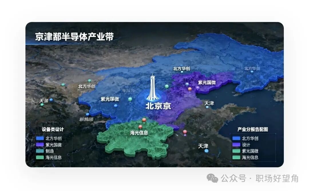
– Beijing: North Huachuang (semiconductor equipment), Unisoc (chip design), Cambricon (AI chip design)
– Tianjin: Haiguang Information (CPU design), Zhonghuan Leading (semiconductor materials)
3. Pearl River Delta: Focusing on Automotive and Communication Chips
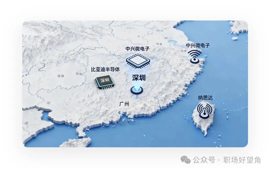
– Shenzhen: BYD Semiconductor (automotive chips), ZTE Microelectronics (communication chips)
– Zhuhai: Nexperia (printer chips), Guangzhou Yuexin Semiconductor (wafer manufacturing)
4. Emerging Industrial Zones: New Growth Points with Unique Processes
– Hefei: Jinghe Integration (wafer manufacturing), Changxin Storage (storage chips)
– Chengdu: Chengdu Huamei (military chips), Silan Jike (wafer manufacturing)
– Xi’an: Yuanjie Technology (optical chips), China Electronics Technology Group 24th Research Institute (semiconductor devices)
3. Job Search Strategies for All Ages: Precise Positioning at Different Stages, Career Development Without Getting Lost
The semiconductor industry covers multiple dimensions including technology, management, and operations. Job seekers of different ages can accurately enter based on their strengths and develop differentiated career plans:
1. Ages 18-30: Entry Period, Solidifying Foundations + Accumulating Experience
– Suitable Positions: Packaging testing technician, equipment maintenance position, process assistant, semiconductor materials sales assistant
– Representative Companies & Salaries: JCET, Wuxi Shenghe, Tongfu Microelectronics, monthly salary 6-10k, some positions include overtime pay + performance bonuses
– Job Search Tips: Highlight internship experience or basic skills (such as electrician certification, AutoCAD operation), obtain semiconductor packaging engineer and equipment operation certifications; resumes should emphasize learning ability and stress resistance, as the semiconductor industry often involves shift work.
– Career Planning: Focus on one segmented area (such as packaging process, equipment maintenance) within 2-3 years, accumulate mass production project experience, and then consider switching to major companies like SMIC or Changxin Storage, or upgrading to process engineer or equipment engineer roles.
2. Ages 30-35: Growth Period, Technical Breakthroughs + Management Advancement
– Suitable Positions: Core R&D positions, technical supervisors, project leaders, chip design engineers
– Representative Companies & Salaries: SMIC, Cambricon, North Huachuang, monthly salary 15-30k, some R&D positions include project bonuses + equity incentives
– Job Search Tips: Highlight project achievements (such as “participated in the mass production of XX chip, improving yield by 10%”), showcase technical expertise (such as mastering FinFET technology, Chiplet packaging technology); candidates with cross-departmental collaboration abilities and project management experience are preferred.
– Career Planning: Focus on high-growth areas such as AI chips, power semiconductors, and advanced packaging, developing towards technical expert or technical management roles; consider obtaining certifications such as Synopsys certified IC designer, senior semiconductor equipment engineer, etc., to enhance industry recognition.
3. Ages 35-40: Stability Period, Resource Integration + Deepening Segmentation
– Suitable Positions: Technical directors, production plant managers, regional sales managers, semiconductor industry consultants
– Representative Companies & Salaries: Hua Hong Semiconductor, Silan Microelectronics, Jinghe Integration, monthly salary 25-50k, some management positions include year-end bonuses
– Job Search Tips: Highlight industry resources (such as supply chain resources, customer resources) and mature project experience (such as “led the expansion project of XX wafer factory”); emphasize risk resistance and strategic thinking, as the semiconductor industry is significantly affected by geopolitical factors.
– Career Planning: Deepen expertise in a specific segment (such as power semiconductors, semiconductor equipment) to become an expert in the field; consider transitioning to enterprise management, strategic planning, or industry consulting roles to mitigate the risk of job loss due to technological iterations.
4. Ages 40 and Above: Transition Period, Reusing Experience + Cross-Industry Collaboration
– Suitable Positions: Supporting roles in the semiconductor industry chain (such as supply chain management, quality control, industry training), technical consultants for upstream and downstream companies
– Representative Companies & Salaries: Semiconductor equipment agents, automotive parts companies (chip-related businesses), industry training institutions, monthly salary 15-30k, high job stability
– Job Search Tips: Highlight the reusability of industry experience (such as “semiconductor quality management experience can be transferred to automotive chip quality inspection”), showcase cross-industry collaboration abilities; resumes should emphasize resource integration and problem-solving skills.
– Career Planning: Utilize semiconductor industry experience to enter upstream and downstream fields such as automotive, IoT, and new energy for a smooth transition; consider starting a business or joining a startup as a technical consultant or operations manager.
4. Tips for Outsiders Transitioning into the Industry: 3 Entry Directions + 4 Preparation Steps, Zero Foundation Can Also Enter
Although the semiconductor industry has high technical barriers, it is not “out of reach”. Outsiders can enter through low-threshold positions and gradually achieve career transformation:
1. 3 Low-Threshold Entry Directions
– Direction 1: Basic Operation Positions: Packaging testing technicians, equipment maintenance positions, cleanroom operators in wafer factories, with low professional background requirements, and companies provide systematic training.
– Direction 2: Auxiliary R&D Positions: Project assistants in chip design service companies, laboratory assistants in semiconductor materials companies, allowing exposure to core business and accumulation of industry experience.
– Direction 3: Supporting Roles in the Industry Chain: Semiconductor exhibition planning, supply chain management, sales assistants, industry media editors, leveraging existing skills (such as sales, planning, writing) to cross into the industry.
2. 4 Steps for Transition Preparation
– Step 1: Supplement Core Knowledge: Learn basic semiconductor terminology and industry chain logic through online courses (such as Coursera semiconductor courses, Bilibili “Semiconductor Industry Observation”); focus on mastering vacuum basics, semiconductor manufacturing processes, and introductory chip design knowledge.
– Step 2: Obtain Practical Certifications: Prioritize obtaining semiconductor packaging engineer, equipment operation certifications, Synopsys certified IC designer (entry-level) to enhance resume competitiveness.
– Step 3: Accumulate Project Experience: Participate in RISC-V open-source chip projects, EETOP forum virtual projects, or seek semiconductor-related part-time jobs on platforms like Xianyu and GitHub to compensate for the lack of industry experience.
– Step 4: Expand Industry Connections: Connect with industry professionals on LinkedIn, join semiconductor industry WeChat groups, attend industry exhibitions like SEMICON China to gain internal referral opportunities.
3. 3 Key Considerations
– Maintain Lifelong Learning: Semiconductor technology iterates quickly, requiring continuous tracking of cutting-edge technology trends such as CFET and High-NA EUV to avoid being eliminated from the industry.
– Assess Enterprise Risk Resistance: Before joining, understand whether the enterprise has stable orders, technical reserves, and policy support, avoiding companies overly reliant on a single customer or technology.
– Reject “One-Step Completion”: Outsiders should not blindly pursue high-end positions such as chip design or advanced process R&D start from basic positions, gradually accumulate experience before upgrading.
The semiconductor industry is in the golden decade of domestic substitution, with abundant opportunities in both technical and supporting positions. However, behind these opportunities, job seekers need solid professional skills, a continuous learning mindset, and a clear career plan.
If you are preparing to enter the semiconductor industry, consider your age and strengths to find the right entry direction; if you are already deep in the industry, feel free to share your job search experiences and career insights in the comments to help others avoid detours!
Finally, don’t forget to save and share this guide with friends who want to learn about the semiconductor industry, and together seize the industry dividends for a career leap~
#SemiconductorIndustry #JobSearchStrategies #DomesticSubstitution #CareerPlanning #CrossIndustryTransition
Image Note: Some images are from the “Industry Research Report WeChat Public Account”.