The following are key considerations to keep in mind when processing RF antenna PCBs, covering all aspects from material selection to specific process requirements:
1. PCB Substrate Selection
This is the most critical foundation; if the wrong material is chosen, subsequent processes cannot compensate for it.
1. Low Loss High-Frequency Materials:
It is essential to use: standard FR-4 material can handle low frequencies (e.g., <1GHz), but at higher frequencies (e.g., 2.4GHz, 5GHz), losses will be significant, severely affecting antenna efficiency and gain.
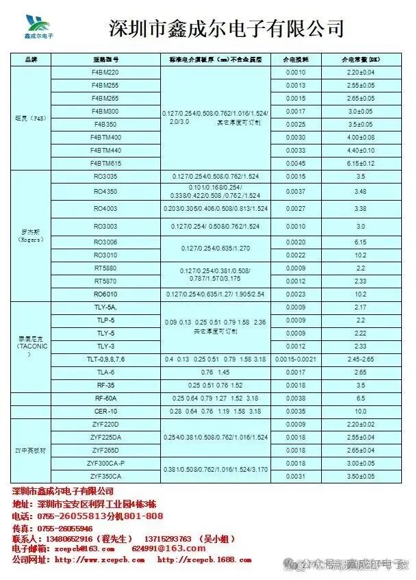
Common materials include:Rogers series RO4003C, RO4350B, Taconic TLY/TLY-5, Isola IS680, etc.. These materials have stable and low dielectric constants and very low loss factors.
Selection criteria: Choose based on operating frequency, cost budget, and performance requirements. RO4350B is a good balance between cost and high performance.
2. Stability of Dielectric Constant:
The dielectric constant of high-frequency materials should vary little with temperature and frequency. This ensures consistent antenna performance in different environments.
3. Copper Foil Type:
Prefer low profile or reverse treated copper foil. Standard rough copper foil surfaces will increase conductor losses at high frequencies (skin effect).
2. Processing Precision and Process Requirements
1. Impedance Control:
Clear requirements: Impedance requirements (e.g., 50Ω single-ended impedance) and the lines that need to be controlled (e.g., microstrip, coplanar waveguide) must be clearly marked on the Gerber files or processing drawings.
Provide stacking information: Provide the PCB manufacturer with complete stacking structure information, including the dielectric thickness, copper thickness, and dielectric constant for each layer. The manufacturer will calculate and adjust the line width and spacing to achieve the target impedance based on this information.
Request impedance test reports: A reputable RF PCB manufacturer will provide impedance test reports after production, proving that the processing meets impedance control requirements.
2. Etching Precision and Consistency:
The shape of the antenna and the width of the feed line are core determinants of its performance. Etching must be precise and uniform, with smooth and vertical edges.
Rough etching edges will increase resistance and parasitic effects, altering the effective electrical length of the antenna, leading to frequency shifts.
Confirm the manufacturer’s line width tolerance capability; typically, excellent manufacturers can achieve ±0.02mm or better.
3. Dielectric Layer Thickness Control:
The thickness of the dielectric layer directly affects impedance and the coupling between the antenna and the ground plane. Thickness tolerances must be strictly controlled.
During stacking design, confirm the thickness specifications of the core board and prepreg with the manufacturer, and choose materials with small tolerances.
4. Surface Treatment:
Gold immersion is preferred: Chemical nickel immersion gold has the advantages of a flat surface, good solderability, low and stable contact resistance, making it the first choice for RF circuits.
Be cautious with tin spraying: The uneven surface of tin spraying leads to significant losses for high-frequency signals, which is not conducive to fine mounting and is not recommended for RF circuits.
OSP: Can be considered in cost-sensitive and low-frequency situations, but its performance and protection of non-solder areas are inferior to gold immersion.
Silver paste: Used in certain specific situations, but may pose migration risks.
5. Via Technology:
Ground vias: For ground holes around coplanar waveguides or microstrip lines, they must be full and void-free. Typically, electroplated filled holes or resin-filled holes are required to prevent energy leakage and mode coupling.
Via positioning: Ground vias should be as close as possible to signal vias or transmission lines to provide the shortest return path.
3. Design and Communication
1. Provide a complete process requirements document:
* Create a separate “PCB Process Requirements” document that clearly lists:
* Material model (e.g., Rogers RO4350B)
* Final board thickness and tolerances
* Impedance control values and corresponding line widths (indicate 50Ω microstrip, etc.)
* Copper thickness requirements
* Surface treatment processes (e.g., gold immersion, thickness requirements)
* Solder mask and silkscreen requirements (RF traces and antenna areas usually do not require solder mask coverage)
* Any special requirements (e.g., mixed lamination: RO4350B + FR-4)
2. Communicate with the manufacturer in advance:
Do not just send the Gerber files and be done with it. Before submitting the board, be sure to communicate your design with the manufacturer’s engineers, especially regarding impedance control and material requirements.
Confirm that the manufacturer has experience and capability in processing high-frequency boards. You can ask them about commonly used high-frequency material brands, minimum line width/spacing, impedance control capabilities, etc.
3. Consider “core stealing” techniques:
When using expensive high-frequency core materials like Rogers in conjunction with FR-4, to save costs, you can hollow out the expensive material in non-RF areas, leaving only the part under the RF circuit. This requires detailed discussion with the manufacturer about design and process feasibility.
4. Other Considerations
Cleanliness:PCBs must be thoroughly cleaned after processing to ensure no ionic contamination, as this will affect the long-term reliability of RF performance.
Solder Mask Windows:In critical areas such as antenna radiators and RF transmission lines, solder mask windows are usually required, meaning no solder mask ink coverage. This is because the dielectric constant of solder mask ink is uncertain and can affect performance.
Board warping: High-frequency materials are usually quite rigid, but care must also be taken to control flatness after processing.
Summary Points (Checklist for the Manufacturer)
When communicating with the PCB manufacturer, you can directly provide the following points:
1. Material: Use Rogers RO4350B (or other specified high-frequency materials).
2. Impedance: Control XX ohm impedance, corresponding line widths refer to drawings/files, please adjust according to your process and provide impedance test reports.
3. Etching: Require smooth line edges, with line width tolerances strictly controlled within ±0.02mm.
4. Surface Treatment: Chemical gold immersion.
5. Vias: Ground vias require electroplated filled holes/full.
6. Solder Mask: Solder mask windows for RF traces and antenna areas.
7. Cleanliness: High standard cleaning required, low ionic contamination.
By strictly controlling the above aspects, the RF antenna PCB produced can best match the performance of your simulation design.