
[Click on the public account above]
 ▲Get a free collection of learning tools▲
In PCB design, pads are a very important concept, and PCB engineers are certainly familiar with them. However, despite their familiarity, many engineers have only a partial understanding of pads.
Today, let’s explore the types of pads and the design standards for pads in PCB design.Pads are the basic building blocks of surface mount assembly, used to form the pad pattern (land pattern) of the circuit board, which is a combination of pads designed for various special component types. Pads are used for electrical connections, device fixation, or both, and are part of the conductive pattern.

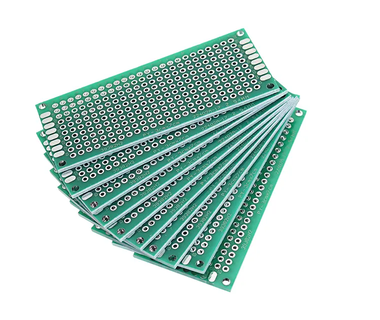
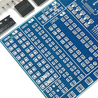
Types of PCB Pads1. Common Pads1. Square Pads – Often used when components on the printed circuit board are large and few, and the printed wiring is simple. This type of pad is easy to implement when manually creating PCBs.
2. Round Pads – Widely used in single and double-sided printed circuit boards with regular component arrangements. If the board density allows, the pads can be larger to prevent detachment during soldering.
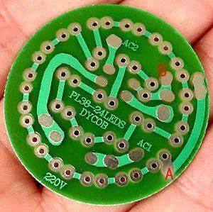
3. Island Pads – The connections between pads are integrated. Commonly used in vertical irregular arrangements.
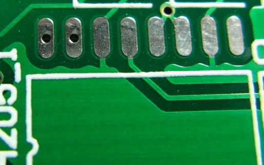
4. Polygonal Pads – Used to distinguish pads with similar outer diameters but different hole diameters, facilitating processing and assembly.5. Oval Pads – These pads have sufficient area to enhance peel strength and are commonly used for dual in-line package devices.
6. Open Pads – Commonly used to ensure that the pad holes for manual rework are not sealed by solder after wave soldering.2. Special Pads1. Star Pads
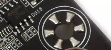
Star pads are typically used in large through-hole grounding positions. The design has the following reasons:1) The fixed hole needs to be metallized and connected to GND. If the fixed hole is fully metallized, it can easily get blocked during reflow soldering.2) Using internal metal screw holes may lead to poor grounding due to installation or repeated disassembly. However, using star pad designs can ensure good grounding regardless of stress changes.2. Cross Pads

Cross pads, also known as thermal pads or hot air pads, serve to reduce heat dissipation from the pad during soldering, preventing cold solder joints or PCB delamination due to excessive heat.1) When your pad is a ground line, the cross can reduce the area connected to the ground line, slowing down the heat dissipation rate, making soldering easier.2) When your PCB requires machine placement and is using a reflow soldering machine, cross pads can prevent PCB delamination (as more heat is needed to melt solder paste).3. Teardrop Pads
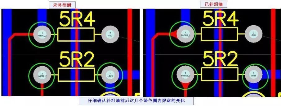
Teardrop pads are often used when the traces connected to the pads are thin, to prevent pad delamination and disconnection from the traces. This type of pad is commonly used in high-frequency circuits.Design Standards for Pads in PCB Design1. Design Standards for the Shape and Size of PCB Pads:1) Use the standard PCB package library.2) The minimum single-sided pad width should not be less than 0.25mm, and the maximum diameter of the entire pad should not exceed three times the component hole diameter.3) Ensure that the edge distance between two pads is greater than 0.4mm.4) Pads with a hole diameter greater than 1.2mm or a pad diameter greater than 3.0mm should be designed as diamond or star-shaped pads.5) In cases of dense wiring, it is recommended to use oval or elongated connection pads. The diameter or minimum width of single-sided pads should be 1.6mm; for double-sided boards, the weak signal line pads only need a hole diameter plus 0.5mm, as overly large pads can lead to unnecessary solder bridging.2. Standards for Pad Hole Sizes:The inner hole of the pad should generally not be less than 0.6mm, as holes smaller than 0.6mm are difficult to process during mold punching. Typically, the inner hole diameter of the pad is the metal pin diameter plus 0.2mm. For example, if the metal pin diameter of a resistor is 0.5mm, the corresponding inner hole diameter of the pad would be 0.7mm, and the pad diameter depends on the inner hole diameter.
3. Key Points for Reliability Design of PCB Pads:1) Symmetry: To ensure the surface tension of molten solder is balanced, the pads at both ends must be symmetrical.2) Pad Spacing: Too large or too small spacing between pads can lead to soldering defects, so it is important to ensure appropriate spacing between component leads or pins and pads.3) Remaining Pad Size: The remaining size after the component lead or pin overlaps with the pad must ensure that a solder joint can form a convex surface.4) Pad Width: Should be roughly consistent with the width of the component lead or pin.
~END~
This article is edited and reprinted for the purpose of conveying more information and does not represent the views of this website or its authenticity. Copyright belongs to the original author. If there are any issues regarding the content, copyright, or other matters, please contact this public account within 30 days WeChat (kunyi346416), and we will delete the content as soon as possible! ▼Click the link below to follow the recommended public account▼

 ●[Technical Articles]Several typical mistakes made by hardware engineers have been compiled and posted for everyone●[Technical Article] Power engineers have no “money” path? Perhaps you haven’t found the right direction●[Collection of Useful Information] Collection | Comprehensive PCB Production Process●[Useful Materials] 104 PCB Design Tips Q&A | Worry-free Board Design!●[Technical Content] Is learning PADS enough? A complete collection of non-mold commands●[Material Sharing] Planning to enroll 200 students for free high-speed PCB learning

If you find the content good, please give it a thumbs up!