Copper pouring is an important aspect of Jialichuang’s high-density PCB design. The significance of copper pouring lies in reducing ground line impedance, enhancing anti-interference capability; lowering voltage drop, improving power efficiency; and connecting with the ground line to reduce loop area.
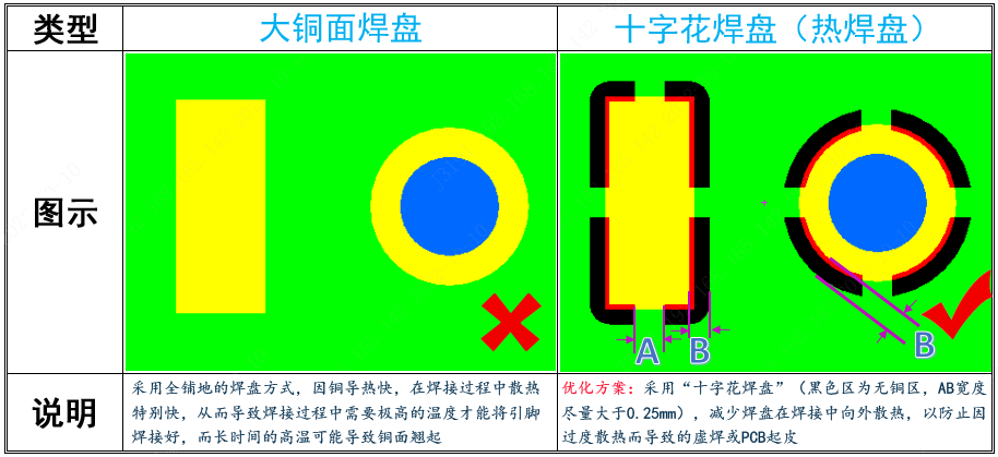
It is advisable to use cross pads on copper pouring surfaces
We know that copper has a high thermal conductivity (approximately 380W), therefore whether it is manual soldering or reflow soldering, the copper surface will quickly conduct heat during soldering, causing temperature loss from the soldering iron, which affects the soldering process. Hence, the design should preferably use “cross pads” to minimize heat dissipation and facilitate soldering.
Selection of Copper Pouring Method
In high-frequency situations, the distributed capacitance of the wiring on the printed circuit board will come into play. When the length exceeds 1/20 of the corresponding wavelength of the noise frequency, an antenna effect will occur, and noise will be emitted through the wiring. If there is poorly grounded copper pouring in the PCB, it becomes a tool for propagating noise. Therefore, in high-frequency circuits, do not assume that grounding a certain point of the ground line constitutes a “ground line”; it must be spaced less than λ/20. Through-holes in the wiring should be well grounded to the ground plane of the multilayer board. If the copper pouring is handled properly, it not only increases current capacity but also provides dual shielding against interference.
Copper pouring generally has two basic methods: large area copper pouring and grid. Large area copper pouring has the dual effect of increasing current and shielding, but during wave soldering, the board may warp or even bubble. Therefore, large area copper pouring usually has several slots to alleviate copper foil bubbling. Pure grid copper pouring primarily serves a shielding function, with the effect of increasing current being reduced. From a heat dissipation perspective, grid pouring is beneficial as it reduces the heated surface of the copper and provides some electromagnetic shielding. With the increasing precision of PCBs and higher quality requirements, most PCB factories have abandoned low-cost wet film processes in favor of superior dry film processes. Therefore, where design allows, minimize grid copper pouring to reduce the impact of dry film fragments on the circuit, and using solid copper pouring is a better method.
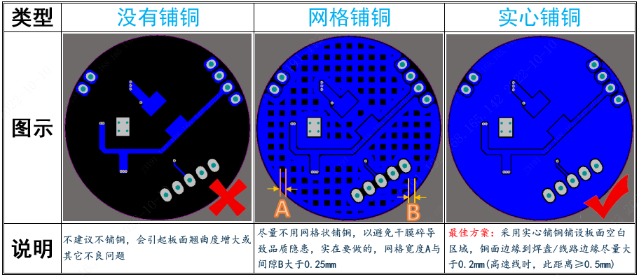
The Importance of Copper Pouring in Open Areas
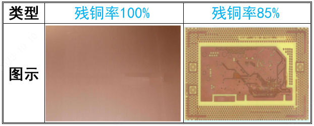
Residual copper rate: refers to the percentage of the inner layer circuit pattern occupying the entire board area. Residual copper rate = area with copper on the current layer / total area of the board. Lamination: multilayer board lamination involves cutting PP into sheets, placing them between the inner core board and the core board or between the core board and copper foil, and then using a press at high temperature and pressure to melt the resin on the PP and fill the non-copper areas of the core board. After cooling, the resin solidifies, bonding the core board and copper foil together. Design defects: if the residual copper rate of the inner layer circuit is too low, the area filled with resin increases, which can lead to the board being too thin, copper foil wrinkling, lack of adhesive causing white spots, delamination, and other issues. Design recommendations: copper foil should be applied to open areas within the board as much as possible, and if there are high-speed signal lines, maintain a distance of more than 0.5mm from the signal lines.

In summary, the core of Jialichuang’s high-density PCB copper pouring lies in “targeted design”: solid copper pouring is prioritized for low-frequency high-current scenarios to ensure current carrying and shielding; grid copper pouring is required for high-frequency circuits in conjunction with dense grounding vias to avoid antenna effects; and the inner layer design must pay attention to the residual copper rate to avoid lamination defects caused by open areas. When designers incorporate soldering convenience, EMI shielding, and lamination reliability into the copper pouring scheme, they can create high-density PCB products that balance performance and quality.