 Noise issues are four words that every circuit board designer will hear. To solve noise problems, it often takes hours of laboratory testing to identify the culprit, only to find that the noise is caused by improper layout of the switching power supply. Addressing such issues may require designing a new layout, leading to product delays and increased development costs.
This article will provide guidelines on printed circuit board (PCB) layout and wiring to help designers avoid such noise issues. Using the dual-channel synchronous controller ADP1850 as an example, the first step is to determine the current path of the regulator. Then, the current path determines the placement of components in this low-noise layout design.
PCB Layout and Wiring Guidelines
Step 1: Determine the Current Path
In switching converter designs, high current paths and low current paths are very close to each other. The AC path carries spikes and noise, while the high DC path can produce significant voltage drops, and low current paths are often sensitive to noise. The key to proper PCB layout and wiring is to identify critical paths, then arrange components and provide sufficient copper area to prevent high current from damaging low current. Poor performance manifests as ground bounce and noise injection into the IC and the rest of the system.
Figure 1 shows a synchronous buck regulator design, which includes a switching controller and the following external power components: high-side switch, low-side switch, inductor, input capacitor, output capacitor, and bypass capacitor. The arrows in Figure 1 indicate the direction of high switch current. Care must be taken to place these power components to avoid generating excessive parasitic capacitance and inductance, which can lead to excessive noise, overshoot, ringing oscillations, and ground bounce.
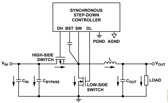
Figure 1. Typical Switching Regulator (showing AC and DC current paths)
Switching current paths such as DH, DL, BST, and SW must be properly arranged after leaving the controller to avoid excessive parasitic inductance. The high δI/δt AC switching pulse current carried by these lines can exceed 3 A and last for several nanoseconds. The high current loop must be kept small to minimize output ringing oscillations and avoid picking up additional noise.
Low-value, low-amplitude signal paths, such as compensation and feedback components, are sensitive to noise. These paths should be kept away from switching nodes and power components to avoid injecting interference noise.
Step 2: Layout Physical Planning
PCB physical planning (floor plan) is very important; it must minimize the area of current loops and reasonably arrange power components to allow smooth current flow, avoiding sharp corners and narrow paths. This will help reduce parasitic capacitance and inductance, thereby eliminating ground bounce.
Figure 2 shows the PCB layout of a dual-output buck converter using the ADP1850 switching controller. Note that the layout of power components minimizes the area of current loops and parasitic inductance. The dashed lines indicate high current paths. This physical planning technique can be used for both synchronous and asynchronous controllers. In asynchronous controller designs, a Schottky diode replaces the low-side switch.
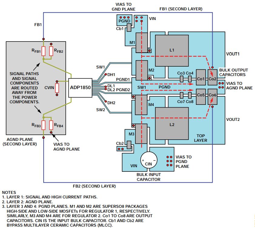
Figure 2. PCB layout of a dual-output buck converter using the ADP1850 controller
Step 3: Power Components – MOSFETs and Capacitors (Input, Bypass, and Output)
The current waveforms at the top and bottom power switches are pulses with very high δI/δt. Therefore, the paths connecting each switch should be as short as possible to minimize noise picked up by the controller and noise transmitted through inductive loops. When using a pair of DPAK or SO-8 packaged FETs on one side of the PCB, it is best to rotate the two FETs in opposite directions so that the switching node is on one side of the pair of FETs, and use appropriate ceramic bypass capacitors to bypass the high-side leakage current to the low-side source. Be sure to place the bypass capacitors as close to the MOSFETs as possible (see Figure 2) to minimize the inductance around the loop through the FET and capacitor.
The placement of input bypass capacitors and large input capacitors is crucial for controlling ground bounce. The negative terminal of the output filter capacitor should be connected as close as possible to the source of the low-side MOSFET, which helps reduce the loop inductance that causes ground bounce. Cb1 and Cb2 in Figure 2 are ceramic bypass capacitors, with recommended values ranging from 1 μF to 22 μF. For high current applications, an additional larger filter capacitor should be paralleled, as shown by CIN in Figure 2.
Thermal Considerations and Ground Layers
Under heavy load conditions, the equivalent series resistance (ESR) of power MOSFETs, inductors, and large capacitors generates a lot of heat. To effectively dissipate heat, the example in Figure 2 places large areas of copper beneath these power components.
Multilayer PCBs have better thermal performance than 2-layer PCBs. To improve thermal and conductive performance, 2 oz copper thickness should be used on a standard 1 oz copper layer. Multiple PGND layers connected together by vias will also help. Figure 3 shows a 4-layer PCB design with PGND layers distributed on the top layer, third layer, and fourth layer.
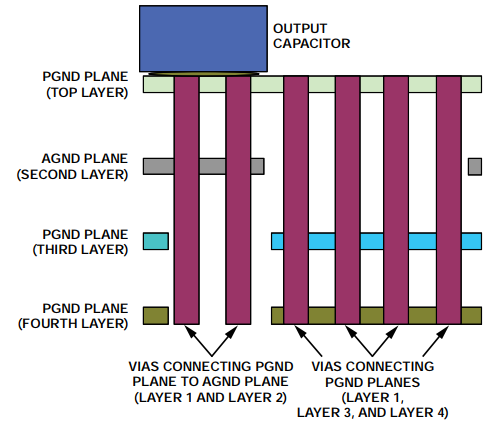
Figure 3. Cross-section: Connecting PGND layers to improve heat dissipation
This multi-ground layer approach can isolate noise-sensitive signals. As shown in Figure 2, the negative terminals of compensation components, soft-start capacitors, bias input bypass capacitors, and output feedback divider resistors are all connected to the AGND layer. Do not directly connect any high current or high δI/δt paths to the isolated AGND layer. AGND is a quiet ground layer with no large currents flowing through it.
All power components (such as low-side switches, bypass capacitors, input and output capacitors, etc.) connect their negative terminals to the PGND layer, which carries high current.
The voltage drop within the GND layer can be significant enough to affect output accuracy. Connecting the AGND layer to the negative terminal of the output capacitor with a wide trace (see Figure 4) can significantly improve output accuracy and load regulation.
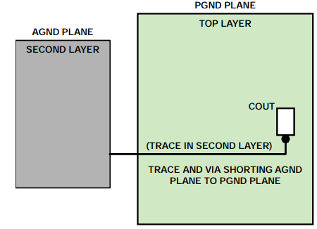
Figure 4. Connection from AGND layer to PGND layer
The AGND layer extends to the output capacitor, and the AGND layer and PGND layer connect at the negative terminal of the output capacitor through vias.
Figure 2 shows another technique for connecting AGND and PGND layers, where the AGND layer connects to the PGND layer through vias near the negative terminal of the large output capacitor. Figure 3 shows a cross-section at a certain location on the PCB where the AGND layer and PGND layer are connected through vias near the negative terminal of the large output capacitor.
Current Sensing Path
To avoid accuracy degradation caused by interference noise, the layout of the current sensing path in current mode switching regulators must be proper. Dual-channel applications require particular attention to eliminate any crosstalk between channels.
The dual-channel buck controller ADP1850 uses the on-resistance RDS(ON) of the low-side MOSFET as part of the control loop architecture. This architecture detects the current flowing through the low-side MOSFET between the SWx and PGNDx pins. Ground current noise in one channel may couple into the adjacent channel. Therefore, it is essential to keep the SWx and PGNDx traces as short as possible and place them close to the MOSFET for accurate current sensing. Connections to the SWx and PGNDx nodes must use Kelvin sensing techniques, as shown in Figures 2 and 5. Note that the corresponding PGNDx trace connects to the source of the low-side MOSFET. Do not arbitrarily connect the PGND layer to the PGNDx pin.
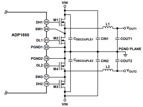
Figure 5. Grounding techniques for two channels
In contrast, for dual-channel voltage mode controllers like the ADP1829, the PGND1 and PGND2 pins are directly connected to the PGND layer through vias.
Feedback and Current Limit Sensing Paths
The feedback (FB) and current limit (ILIM) pins are low signal level inputs, making them sensitive to capacitive and inductive noise interference. FB and ILIM traces should avoid being close to high δI/δt traces. Care should be taken to avoid forming loops in the traces, which can lead to increased undesirable inductance. Adding a small MLCC decoupling capacitor (such as 22 pF) between the ILIM and PGND pins helps further filter out noise.
Switch Node
In switching regulator circuits, the switch (SW) node is the noisiest place because it carries significant AC and DC voltage/current. This SW node requires a large area of copper to minimize resistive voltage drop. Placing the MOSFETs and inductors close to each other on the copper layer can minimize series resistance and inductance.
Applications that are more sensitive to electromagnetic interference, switch node noise, and ringing oscillations can use a small snubber. The snubber consists of a resistor and capacitor in series (see RSNUB and CSNUB in Figure 6), placed between the SW node and the PGND layer, which can reduce ringing oscillations and electromagnetic interference at the SW node. Note that adding a snubber may slightly decrease overall efficiency by 0.2% to 0.4%.
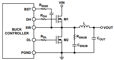
Figure 6. Snubber and gate resistor
Gate Driver Path
The gate drive traces (DH and DL) also handle high δI/δt, often resulting in ringing oscillations and overshoot. These traces should be as short as possible. It is best to route them directly, avoiding the use of vias. If vias must be used, each trace should use two vias to reduce peak current density and parasitic inductance.
Placing a small resistor (about 2 Ω to 4 Ω) in series on the DH or DL pin can slow down the gate drive, thereby reducing gate noise and overshoot. Additionally, a resistor can also be connected between the BST and SW pins (see Figure 6). During layout, leaving space for a 0 Ω gate resistor can improve flexibility for future evaluations. The added gate resistor will extend the rise and fall times of the gate charge, resulting in increased switching power loss in the MOSFET.
Conclusion
Understanding the current paths, their sensitivities, and proper component placement is key to eliminating noise issues in PCB layout design. All power device evaluation boards from ADI follow the above layout and wiring guidelines to achieve optimal performance. Evaluation board documents UG-204 and UG-205 detail the layout and wiring related to the ADP1850.
Note that all switching power supplies have the same components and similar current path sensitivities. Therefore, the guidelines illustrated using the ADP1850 as an example for current mode buck regulators also apply to voltage mode and/or boost switching regulator layout and wiring.