Power Grid Design for Advanced SoCs (TechInsights Analysis Report, January 21, 2025, Author: Tom Dillinger)IntroductionThe development of advanced SoC chip design requires extensive upfront project planning, from market research to technology selection, engineering resource allocation, and the EDA methods employed. A key aspect of this planning work is the implementation of the power/ground distribution network into the SoC (referred to as PDN: Power Distribution Network), which encompasses all these areas.The market has expectations regarding the cost management of PDN systems, from power supply to SoC packaging. The market will also impose strict reliability requirements on products based on the predicted Failures In Time (FIT).The technical selection review conducted with foundries addresses the power versus performance trade-offs when selecting power voltages. This planning discussion must also include the limitations of SoC designs implemented by IP providers, from basic cell libraries to more complex cores and interface IPs. Particularly important is the choice of metallization stack, i.e., the number and combination of metal layer process options in the foundry’s back-end-of-line (BEOL) manufacturing.Engineering resources need to be allocated early for chip layout planning to determine chip costs and packaging layout constraints.EDA methods must support physical design construction, physical verification, and electrical analysis of block-level and complete SoC models.In all these cases, the path to implementing the PDN is a critical part of project planning work.Due to several trends in advanced SoC design, the difficulty of these tasks has increased:i. Multiple different PDN networks or power “domains” on-chipDesigns combine unique power supply voltages assigned to different blocks on the chip—these blocks represent different power “domains.” Designers strive to achieve power optimization through performance versus power trade-offs for the blocks, which may necessitate supporting different PDN voltages.CMOS process technology provides a unique capability to vary the power supply voltage of logic circuits across a range of power supply voltages. Foundries and IP providers offer effective electrical models within this range. (Designers need to use “level-shifting” circuits at block-to-block interfaces, where lower VDD domains connect to higher VDD domains.)Particularly noteworthy are the power domains associated with large on-chip SRAM arrays. Due to strict requirements for static leakage power in many SoC designs, SRAM arrays warrant special consideration. SRAM IP providers will establish corresponding “Vmin” domain values.ii. Dynamic Voltage/Frequency Scaling (DVFS) operating modesSpecific module designs may have a set of operating modes where the module’s PDN is dynamically modified—for example, “boost” (higher performance), “throttle” (for reduced thermal power). Power management functional units (or separate PMIC chips) are instructed by operating system software to switch between elements at a set of (frequency, power) operating points.iii. “Sleep” modesAdditional module-level mode options will require more complex PDN implementations. Supporting “sleep” modes requires both power VDD and ground GND networks in the module—for example, “VDD_always_on” and “VDD_internal_gated.” A set of sleepFET transistor switches is inserted between the two. When “on,” these switches provide a low-resistance connection for normal operation. When “off,” the switches effectively disconnect the two, significantly reducing leakage power.iv. I/O circuit interface levelsThe PDN to I/O circuits will undoubtedly differ from the circuits of the internal core. Advanced foundry process technologies have been certified for operation below 1.0V. This reduction in supply voltage is driven by the scaling of device, interconnect, and dielectric material sizes. In contrast, the interface between the SoC and other system electronics may require larger voltage level shifts for reliable communication—for example, 1.2V-1.8V (or higher).The foundry design rules and electrical models for I/O circuit design differ from those used for internal IP. The PDN to I/O requires very unique domain designs to accommodate the potentially large transient currents generated by simultaneously switching output (SSO) driver circuits.Manufacturing and Packaging Technologies and PDNi. Flip-Chip PackagingThe popular packaging technology for advanced SoCs adopts a “flip-chip” orientation. The metallized surface on the top of the chip is covered with a dielectric layer. Large vias are etched into this layer, and a significant number of (spherical) solder balls or recently emerging (pillar) copper pillars are deposited through the vias.The image below shows an example of TechInsights’ reverse engineering team disassembling the Baidu Kunlun 1-T AI processor SoC (from analysis report APE-2312-802), highlighting the aggressive pad sizes achieved using copper pillars for chip-to-package connections.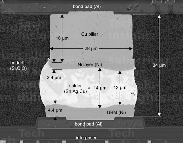 Figure 1 Copper Pillar chip-to-package connection, Baidu Kunlun 1-T chipNote that the footprint of these flip-chip connection technologies aligns very well with the requirements for different PDN domains in the SoC physical design. Specific block domains in chip layout planning will have a PDN “grid” that extends from a single block circuit to a set of different (multiple) bumps/pillars, electrically independent from other domains.ii. Redistribution of BEOL Metal LayersFoundry processes will provide a range of metallization layer combinations, from the densest layers (closest to the circuits) to more relaxed layers (with larger cross-sectional areas and lower resistances), primarily for longer signal interconnect wiring. The requirements of the PDN necessitate metallization that supports (local and global) current density while meeting strict limits on IR voltage drop for the circuits. Advanced SoCs use specific redistribution layer (RDL) metals on the top of the chip to minimize voltage drop (typically made of aluminum rather than copper). RDL patterns provide a transition between bumps/pillars and the PDN domain grid.The cross-section image below is from TechInsights’ analysis of the Samsung Exynos 2400 (from analysis report ACE-2402-802), highlighting the position and relative size of the RDL in the BEOL metallization stack.
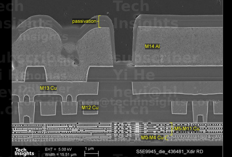 Figure 2 RDL upper layer on BEOL metal ring stack, Samsung Exynos 2400 chipiii. Stacked ViasThe connection from RDL to a (module-level) PDN will utilize vias between the metallization stacked layers. Specifically, the foundry process engineering team will establish design rules and process flows to implement “stacked vias” (sometimes referred to as “super vias”). Stacked vias provide electrical connections across multiple metallization layers in the BEOL configuration. The goal of stacked vias is to provide vertical connections through the metal layers with minimal metal area for each intermediate layer; this helps reduce signal routing channel congestion.The size variations of vias will be limited to maintain an appropriate process window for dielectric etching (without excessive etching). To reduce via resistance, there may be metal overlap regions with (identical) via arrays.iv. PDN Decoupling CapacitorsOn-chip capacitance between the power and ground (P/G) connections of a domain is a key charge source for circuit switching currents. (The inductive impedance between the power supply through the printed circuit board and SoC packaging to the SoC PDN is too large to respond to large fast transient switching currents.) There is a natural capacitance source between power and ground in any circuit layout—for example, between the transistor P/G source nodes and the underlying substrate/well; a fundamental part of PDN design is often to add substrate and well “tap” unit connections from P/G metal to these diffusion nodes. (Well-tap cells are one of the various standard cells analyzed in TechInsights’ SoC design analysis and are part of TechInsights’ Compute products.)These cells are often insufficient to support local capacitance decoupling charge storage requirements. Therefore, additional “decoupling capacitors” are needed as part of the PDN design. Two alternatives are frequently (and widely) used:* Standard CellsThis library cell is inserted into the standard cell row, interleaved with logic cells. Block designers need to evaluate the percentage of area utilization allocated for decoupling capacitor cells in the row based on the expected switching current transients. (The circuits in these cells typically consist of transistors configured such that the Cgs and Cgd of these devices act as capacitance between power and ground.)* Metal-Insulator-Metal (MIM) CapacitorsTo increase manufacturing costs, foundries may offer unique structures embedded in the BEOL metallization stack. An additional (thin) metal layer is fabricated in the dielectric between two conventional BEOL layers. A parallel plate capacitor structure is located between this additional metal layer and the underlying metal. This MIM structure connects to the P/G grid to provide additional local capacitance with high area efficiency.The above image (Note from the translator: This figure 3 is missing in the original report, and the corresponding report for the 7950X3D is also inaccessible) shows the MIM structure, from TechInsights’ analysis of the AMD Ryzen 9 7950X3D manufactured using TSMC’s N7 HPC process (from analysis report ACE-2308-801).Physical Design OptionsAs mentioned in the introduction, PDN implementation decisions are a major part of the initial SoC planning. The “template” of the standard cell library will define the number of lower-level metal routing tracks allocated to the cell rows. The library development team has an inherent definition of this definition:* Tracks allocated to the power and ground “tracks” that run through the template image* Area utilization percentage of logic cells, substrate/well taps, and decap cells* Spacing between higher-level metal P/G grid vias on the tracksThe library development team must make conservative assumptions about the maximum switching activity of logic cells and align with the above utilization and P/G grid assumptions.The SoC physical design team needs to understand these implementation decisions to ensure that their complete P/G grid design meets the requirements.The image below is taken from a recent TechInsights analysis, showing the layout view and SEM view of the standard cell design of the Apple A16 Bionic chip in TSMC’s N4 foundry process, utilizing a “high-density” six-track library template (from analysis report SDA-2211-801).
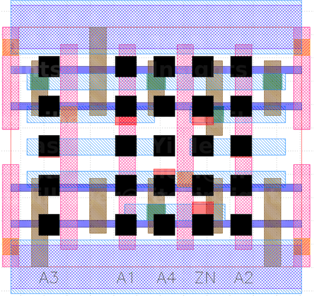 Figure 3 GDS image of high-density standard cells in TSMC N4 process six-track libraryNote that the width of the P/G tracks in the figure is wider than the internal signal lines (e.g., 2X), and the tracks are shared between adjacent cell rows—i.e., the placed cells will be vertically flipped in alternating rows to share VDD and GND track connections with adjacent rows.A similar set of PDN design considerations applies to the integration of hard IP core layouts. IP developers will make assumptions about the connectivity between the IP and the PDN grid. The difference in this case is that the IP will incorporate its own local PDN rather than using the template to “overlay” the P/G tracks.i. P/G “Routing”The physical design of the PDN is somewhat unique because EDA layout and routing toolsets typically provide netlists that describe only signal connections, without power pins. (It is assumed that the P/G template connected to the cell rows will be automatically generated separately from the layout routing process.)Initially, all P/G pins on the layout cells can be viewed as “virtual connections” when confirming signal connections of the physical design using layout-to-netlist tools. This allows block-level physical verification to be independent of other blocks and the global PDN. The final full-chip layout-to-netlist verification needs to ensure that all layout P/G pin connections are correct, including individual domain definitions.Electrical AnalysisOnce the physical design of the power domains is complete, a set of PDN electrical analysis steps will be performed.i. Parasitic Parameter ExtractionThe resistance and capacitance of grid segments and vias are derived from the physical layout by “parasitic parameter extraction” algorithms. This EDA tool interprets the Interconnect Technology File (ITF), which describes the physical thickness and material properties of each metal and dielectric layer.The extracted R and C element netlist includes coordinate information to annotate the load current sources of switching circuits to the parasitic parameter model.The parasitic parameters of RDL and package connections should be incorporated into the overall chip model, which may also include inductive elements.The size of the extracted model’s netlist can become very large, even though the connections between individual nodes in the network are very “sparse.” To achieve more efficient analysis computations, techniques to reduce model size are often employed. Parallel vias can be reduced to a single resistance value. More complex methods are also used to generate summaries of parasitic parameters and current sources for SoC modules and IP cores.ii. IR Voltage Drop AnalysisPerformance characteristics assumptions of library cells and IP cores impose limits on local circuit-level power and ground voltages due to resistive losses in the PDN—for example, VDD drops by “10%” and voltage limits exceed GND.The IR voltage analysis step will add (static or time-dependent) current sources to the PDN network model and perform circuit simulations to confirm that these characteristic limits are not exceeded. Static analysis assumes that load currents are constant over a certain interval and conservatively discards the contribution of capacitive charge delivered to the grid. Dynamic IR analysis is more accurate but also has higher computational requirements. The current sources added to the PDN model reflect time-varying switching transients, requiring careful selection of circuit switching activity.iii. Electromigration AnalysisEach interconnect segment and via in the PDN will be sized during physical design based on the expected current flowing through that segment. It is necessary to confirm these assumptions by simulating the load currents of each element.The manufacturing process ITF, combined with the sizes of each physical element, is used to calculate current density. The reliability of the PDN is then assessed.Each material has a maximum instantaneous current density limit—this can be viewed as a verification that destructive “burnout” events will not occur.Lifetime reliability analysis is also needed to reflect the change in resistivity of elements over time, which is due to the probabilistic nature of electron momentum transfer to metal atoms leading to electromigration of metal atoms.iv. SSO AnalysisThe I/O domain requires special PDN analysis. In this case, more comprehensive package and PCB parasitic models need to be emphasized, as a set of switching I/O driver/receiver current paths cover the connectivity of the entire chip-to-chip interface. Specifically, single-ended parallel bus interfaces need to reflect significant dynamic current transients due to “Simultaneously Switching Outputs” (SSO).FutureSignificant process changes are on the horizon that will affect all aspects of PDN implementation. In upcoming process nodes, PDN networks will transition from top metal resources (competing with signal routing tracks) to the back of the chip, reaching “embedded” power rails directly connected to transistor circuit nodes through (high-density) vias passing through a thinned substrate. In the near future, TechInsights’ analysis of SoCs with BackSide Power Delivery Networks (BSPDN) will provide detailed data on this unique implementation option.