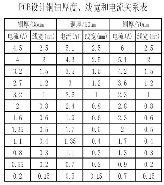
1. The calculation method is as follows: First, calculate the cross-sectional area of the track. Most PCB copper foil thickness is 35um (if unsure, you can ask the PCB manufacturer; 1 ounce is 35um, but it is often less than 35um). The cross-sectional area is obtained by multiplying the trace width by the thickness, and remember to convert to square millimeters. There is an empirical current density value of 15~25 amperes per square millimeter. By multiplying it with the cross-sectional area, we get the current capacity. I=KT0.44A0.75 (K is the correction factor; generally, for internal layers of copper-clad wires, it is taken as 0.024, and for external layers, it is taken as 0.048. T is the maximum temperature rise, measured in degrees Celsius (the melting point of copper is 1060℃). A is the copper cross-sectional area, measured in square MIL (not millimeters, note it is square mil). I is the allowable maximum current, measured in amperes (amp). Generally, 10mil=0.010inch=0.254 can carry 1A, and 250MIL=6.35mm can carry 8.3A.2. Data: The calculation of PCB current carrying capacity has long lacked authoritative technical methods and formulas. Experienced CAD engineers can make accurate judgments based on personal experience. However, for CAD novices, this can be a challenging problem. The current carrying capacity of a PCB depends on the following factors: trace width, trace thickness (copper foil thickness), and allowable temperature rise. Everyone knows that the wider the PCB trace, the greater the current carrying capacity. Here, let me ask you: assuming under the same conditions, if a 10MIL trace can carry 1A, how much current can a 50MIL trace carry? Is it 5A? The answer is naturally no. Please see the data provided by international authoritative organizations: the unit of trace width is: Inch (1 inch = 25.4 millimeters). 1 oz. copper = 35 microns thick, 2 oz. = 70 microns thick, 1 OZ = 0.035mm, 1mil = 10-3 inch. Trace Carrying Capacity per mil std 275.3. Experiment: The experiment also needs to consider the voltage drop caused by the line resistance due to wire length. The solder on the process is only to increase the current capacity, but it is difficult to control the volume of solder. 1 OZ copper, 1mm wide, generally can carry 1-3 A of current, depending on your wire length and voltage drop requirements. The maximum current value should refer to the maximum allowable value under temperature rise limits. The fuse value is the value at which the temperature rise reaches the melting point of copper. Eg. 50mil 1oz temperature rise to 1060 degrees (the melting point of copper), the current is 22.8A.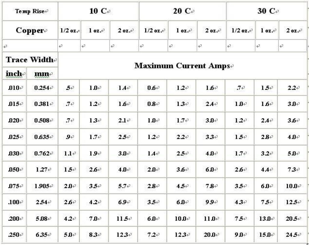 4. The relationship between PCB design copper foil thickness, trace width, and current: Before understanding the relationship between PCB design copper foil thickness, trace width, and current, let us first understand the conversion between the unit ounces, inches, and millimeters for PCB copper foil thickness: “In many data sheets, the copper foil thickness of PCBs is often expressed in ounces, and its conversion relationship with inches and millimeters is as follows: 1 ounce = 0.0014 inches = 0.0356 millimeters (mm) 2 ounces = 0.0028 inches = 0.0712 millimeters (mm) Ounce is a weight unit, and it can be converted to millimeters because the copper foil thickness of the PCB is ounces per square inch.” PCB design copper foil thickness, trace width, and current relationship table.
 The current carrying value of the wire has a direct relationship with the number of vias and pads present (currently, no formula has been found to calculate the impact of pad and via diameter per square millimeter on the line’s carrying capacity; friends interested can look for it themselves; personally, I am not too clear about it; it is not explained here). Here, I will just briefly mention some factors that mainly affect the line’s current carrying capacity. 1. The carrying values listed in the table data are the maximum current carrying values that can be tolerated at a normal temperature of 25 degrees. Therefore, in practical design, various environmental factors, manufacturing processes, board material processes, and board quality must also be considered. Thus, the data provided in the table should only serve as a reference value. 2. In practical design, each wire will also be affected by pads and vias. For example, if a segment of wire has many pads, after soldering, the current carrying capacity of that segment will greatly increase. Many people have seen sections of wire burned out between pads on high current boards; the reason is simple: after soldering, the pads, due to component legs and solder, have enhanced the current carrying capacity of that segment of wire, while the maximum current carrying capacity of the pads between pads will be the maximum current carrying capacity allowed by the wire width. Therefore, during instantaneous fluctuations in the circuit, it is easy to burn out the segment of wire between pads. The solution is to increase the wire width. If the board does not allow increasing the wire width, add a Solder layer to the wire (generally, a 1mm wire can add a Solder layer wire of about 0.6; of course, you can also add a 1mm Solder layer wire). Thus, after soldering, this 1mm wire can be regarded as a 1.5mm~2mm wire (depending on the uniformity and amount of solder during soldering), as shown in the figure below:
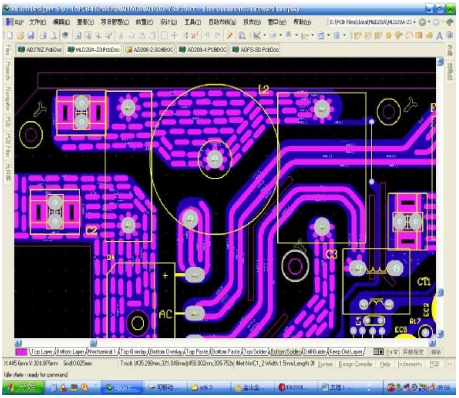 Such methods of handling are not unfamiliar to friends engaged in small appliance PCB Layout. Therefore, if the solder amount is uniform and sufficient, this 1mm wire can be regarded as more than a 2mm wire. This point is particularly important in single-sided high current boards. 3. The processing method around the pads in the figure also increases the uniformity of the current carrying capacity between the wire and the pads, which is particularly important in boards with large current thick pins (pins greater than 1.2, pads greater than 3). This handling is very important. If the pads are over 3mm and the pins are over 1.2, after soldering, the current of that pad can increase dozens of times. If a large current suddenly fluctuates, the current carrying capacity of the entire wire will become very uneven (especially when there are many pads), making it very easy to burn out the wire between pads. The treatment shown in the figure can effectively disperse the uniformity of the current carrying values between a single pad and the surrounding wire. Finally, I would like to reiterate: the current carrying value data table is only an absolute reference value. When not designing for high currents, increasing the amount by 10% based on the values provided in the table will definitely meet design requirements. In general single-sided board design, with a copper thickness of 35um, it can be designed at a basic 1:1 ratio, that is, 1A of current can be designed with a 1mm wire, which can meet the requirements (calculated at a temperature of 105 degrees).5. The relationship between copper foil thickness, trace width, and current in PCB design: The current strength of the signal. When the average current of the signal is large, the current that the wiring width can carry should be considered. The trace width can refer to the following data: The relationship between copper foil thickness, trace width, and current in PCB design. The current carrying capacity of copper foil with different thicknesses and widths is shown in the table below:
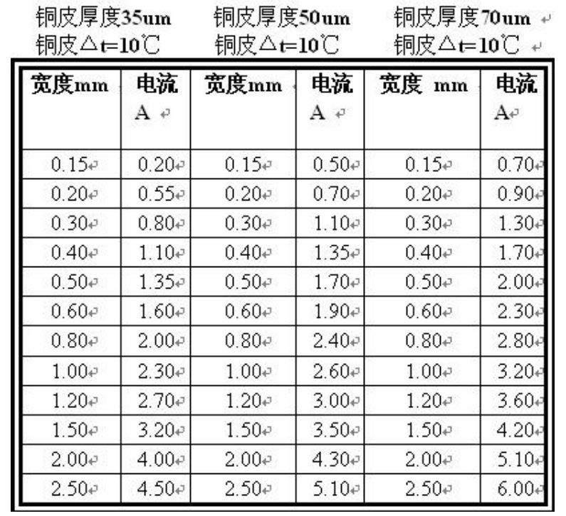 Note: i. When using copper foil as wire to carry large currents, the current carrying capacity of the copper foil width should be selected considering a derating of 50% based on the values in the table. ii. In PCB design and processing, OZ (ounces) is commonly used as the unit of copper foil thickness. The definition of 1 OZ copper thickness is that the weight of copper foil within an area of one square foot is one ounce, corresponding to a physical thickness of 35um; 2OZ copper thickness is 70um. Excerpted from: Huawei PCB Wiring Specification Internal Data P10.6. Empirical formula: I=KT0.44A0.75 (K is the correction factor; generally, for internal layers of copper-clad wires, it is taken as 0.024, and for external layers, it is taken as 0.048. T is the maximum temperature rise, measured in degrees Celsius (the melting point of copper is 1060℃). A is the copper cross-sectional area, measured in square MIL (not millimeters, note it is square mil). I is the allowable maximum current, measured in amperes (amp). Generally, 10mil=0.010inch=0.254 can carry 1A, and 250MIL=6.35mm can carry 8.3A.7. A calculation method provided by a netizen is as follows: First, calculate the cross-sectional area of the track. Most PCB copper foil thickness is 35um (if unsure, you can ask the PCB manufacturer). The cross-sectional area is obtained by multiplying the trace width by the thickness, and remember to convert to square millimeters. There is an empirical current density value of 15~25 amperes per square millimeter. By multiplying it with the cross-sectional area, we get the current capacity.8. Some experience regarding trace width and via copper plating: When drawing PCBs, we generally have a common sense that we use thick lines (e.g., 50mil or even more) for places carrying large currents and thin lines (e.g., 10mil) for small current signals. For certain electromechanical control systems, sometimes the instantaneous current flowing through the traces can reach over 100A; in such cases, relatively thin lines will definitely have issues. A basic empirical value is: 10A per square mm, meaning that a trace with a cross-sectional area of 1 square millimeter can safely carry a current value of 10A. If the trace width is too thin, it can burn out when a large current passes through. Of course, the current burning out the trace must also follow the energy formula: Q=I*I*t. For example, for a trace with a current of 10A, if a current spike of 100A occurs for a duration on the microsecond level, a 30mil trace can definitely withstand it. (At this time, another problem may arise: stray inductance of the trace; this spike will produce a strong back electromotive force under the action of this inductance, which may damage other components. The thinner and longer the trace, the greater the stray inductance, so in practice, the length of the trace must also be considered.) Generally, PCB design software offers several options for copper plating vias on component pins: right-angle spokes, 45-degree spokes, and direct plating. What are the differences? Beginners often do not pay much attention, choosing one at random based on aesthetics. However, it is not so. There are two main considerations: first, it should not dissipate heat too quickly; second, consider the current carrying capacity. The characteristic of using direct plating is that the current carrying capacity of the pads is very strong. For components on high-power circuits, this method must be used. At the same time, its heat dissipation performance is also strong, which is beneficial for component heat dissipation during operation, but this poses a challenge for the PCB soldering personnel, as the pads dissipate heat too quickly, making it difficult to solder, often requiring larger wattage soldering irons and higher soldering temperatures, thus reducing production efficiency. Using right-angle spokes and 45-degree spokes will reduce the contact area between the pins and copper foil, dissipating heat slowly and making soldering easier. Therefore, the choice of connection method for via pads should be based on the application scenario, considering both current carrying capacity and heat dissipation ability. Small power signal lines should not use direct plating, while pads carrying large currents must use direct plating. As for right angles or 45 degrees, it is a matter of aesthetics. Why am I bringing this up? Because I was recently studying a motor driver, and the components in the H-bridge kept burning out. For four or five years, I couldn’t find the cause. After much effort, I finally discovered: it turned out that one component’s pad in the power circuit used a right-angle spoke copper plating method (and due to poor copper plating, only two spokes actually appeared). This greatly reduced the current carrying capacity of the entire power circuit. Although the product had no issues during normal use and operated normally under 10A current, when a short circuit occurred in the H-bridge, a current of about 100A appeared on that circuit, and those two spokes burned out instantly (on the microsecond level). Then, the power circuit became an open circuit, and the energy stored in the motor had no discharge path, dissipating through every possible route, which burned out the current sensing resistor and related operational amplifier components, damaged the bridge control chip, and intruded into the digital circuit part’s signals and power supply, causing severe damage to the entire device. The entire process was as thrilling as using a hair to trigger a big landmine. Copyright statement: The copyright of this article belongs to the original author and does not represent the views of the association. The articles pushed by “Jiangxi Province Electronic Circuit Industry Association” are for sharing purposes only and do not represent the position of this account. If there are copyright issues, please contact us for deletion.