The circuit board cannot do without power chips. We generally use a large capacitor (100μF to 1000μF) and a small capacitor (0.1μF or 0.01μF) as the power filtering capacitors.The large capacitor is used to filter out low-frequency noise, while the small capacitor is used to filter out high-frequency noise.You have designed so many circuit boards; have you placed the capacitors correctly on the circuit board?Let’s first look at a set of PCB diagrams: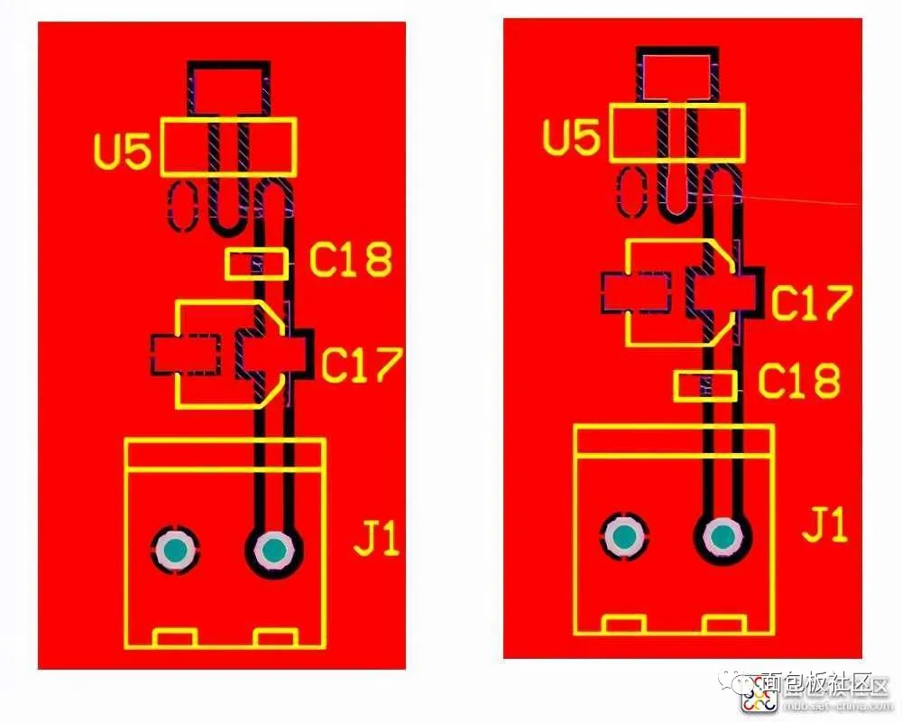 In this diagram, the difference is whether the power positive terminal goes through the large capacitor first or the small capacitor.The correct connection method is:the power positive terminal goes through the large capacitor first, then the small capacitor. (The left diagram is correct)Now let’s look at another set of PCB diagrams:
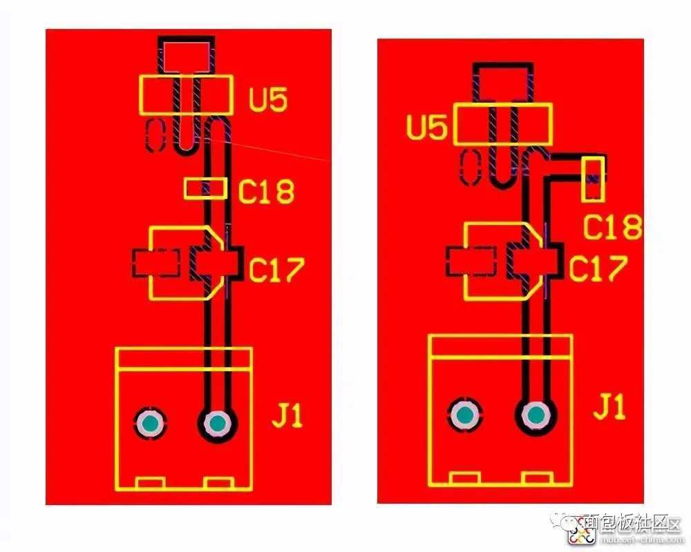 In this diagram, the difference between the left and right diagrams is that the left diagram goes through the large capacitor first, then the small capacitor, while the right diagram goes through the large capacitor first, then the power chip, and connects a small capacitor next to the power chip.The correct connection method is the left diagram.In general situations, either connection method can work, but for high-precision applications, to minimize power noise, it is best to connect according to the correct method described above for optimal filtering effect.
Statement:The copyright of this article belongs to the original author and does not represent the views of the association.The articles promoted by the “Jiangxi Province Electronic Circuit Industry Association” are for sharing purposes only and do not represent the position of this account. If there are any copyright issues, please contact us for removal.