▼ Follow the public account below for more information ▼
In high-voltage PCB design, attention must be paid to electrical clearance and creepage distance in switch mode power supply PCB design; insufficient distance can lead to leakage.
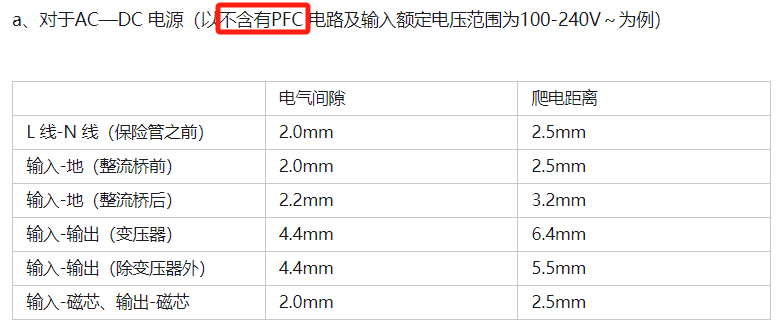
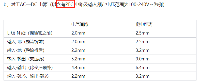
General standards (varying by industry, such as lighting, electric vehicles, etc.) require certified products: design according to standard tables.GB4943.1 corresponds to EC60950.1 (IEC62368-1),GB/T16935.1-2008 corresponds to IEC60664.1 IPC-2221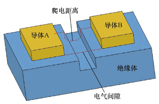
The electrical clearance and creepage distance in PCB design affect electrical performance, safety, and reliability.The electrical clearance and creepage distance are related to voltage, insulation materials (dielectric constant, arc resistance), temperature and humidity, pollution, and conductivity.
| Electrical Clearance | Creepage Distance | |
|---|---|---|
| Defined according to IEC60950 standards | 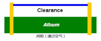 |
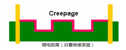 |
| Definition | The shortest path air gap measured between two conductive objects or between a conductive part and the boundary surface of the device through air. | The shortest path creepage distance measured along the surface of the insulating material between two conductive objects. |
| Solutions for Insufficient Clearance | 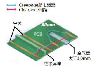 |
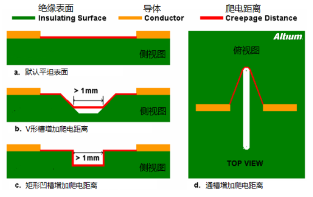 |
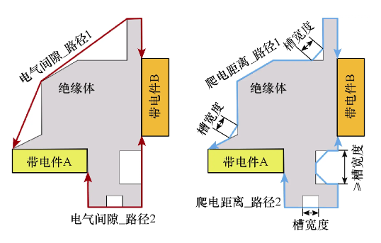
| 1mm Slot Issue | Insufficient electrical clearance; slotting may not necessarily solve the electrical clearance issue. | Slots greater than 1mm can increase surface creepage distance but do not increase electrical clearance. |
Solutions for Insufficient Electrical Clearance
1Implement spacing through insulating materials and, where possible, build on both sides;2High and low voltage isolation, placing high voltage on top and low voltage on the bottom.
Solutions for Sparse Creepage Distance
Figure ashows multilayer surfaces, where creepage distance is measured on the PCB surface between nodes;Figure bshows that V-shaped slots can increase the surface distance between nodes, with the increased length only measured along the coast reducing to a point of 1mm width;Figure cshows multilayer, which can further increase surface distance, but the width must be 1mm or greater, increasing processing costs;Figure dshows direct slots on the PCB, where slots greater than 1mm can hide surface distance, simple and practical.
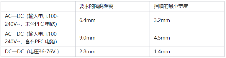
Reference for Electrical Isolation Distance in Electronic Palladium and PCB
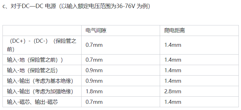
Reference for Electrical Isolation Distance Inside Transformers
The electrical isolation distance inside a transformer refers to the total width of the transformer walls. If the width of the transformer wall is 3mm, then the electrical isolation distance of the transformer equals 6mm (the width of the transformer walls is the same). If there are no walls in the transformer, then the isolation distance equals the thickness of the insulating paper used. Additionally, for AC-DC power supplies, the transformer primary and intermediate structure applies three layers of insulating paper for isolation, while DC-DC power supplies can only use two layers of insulating paper for isolation. The following values do not include margins:
 Note: If the transformer pins are not covered with insulating sleeves, then the isolation distance at the pins may bypass the thickness of the insulating paper and protective walls, so the transformer pins need to be covered with insulating sleeves that must pass through the walls.
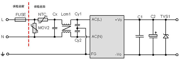
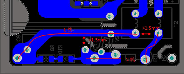 Electrical clearance between L and N lines before the fuse = 2.0mm.Electrical clearance between L and N lines after the fuse = 1.5mm.
Conclusion on 220V Electrical Clearance and Creepage Distance
Electrical clearance > 2mmCreepage distance > 2.5mmIf encountering positions where creepage distance cannot be satisfied, slots > 1mm can meet design requirements and prevent leakage.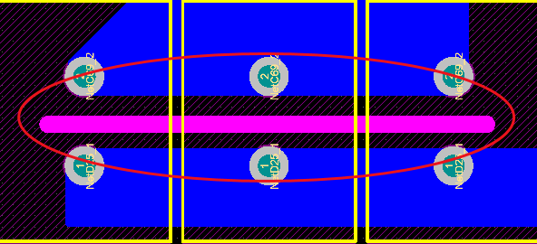
Source: WeChat public account: Electronic Engineer’s Notes