This article explores the design and implementation of a dashcam based on the CAN bus, detailing the overall system structure, hardware circuit design, and software design process. The developed dashcam is used to collect real-time data from the vehicle’s CAN bus during operation and stores the data on a USB drive, which can then be transferred to a PC for analysis using software. This overcomes the previous mode where on-site data collection systems required a computer, allowing for real-time monitoring of various data changes during vehicle operation and synchronously recording driving conditions. After long-term testing or driving, the recorded data can be used to analyze vehicle performance and the operation of various components, facilitating calibration and design work.
1. Overall System Structure Design
Due to the excellent characteristics of the CAN serial communication bus, it is widely used in fields such as on-site data collection systems, automotive manufacturing, and aerospace industries. The CAN bus data logger designed in this article is applied to the Chery A5 model, collecting and storing node data from the entire vehicle’s CAN network. The A5 is the first domestic car brand to use the CAN bus system, primarily applied in the transmission department, with some minor applications in the body, ITS, and information departments. Real-time data collection from the A5, which first utilized CAN technology, is of great significance for understanding various data changes during vehicle operation and for the R&D of the A5 and all subsequent models.
The overall structural diagram of the CAN bus dashcam is shown in Figure 1.
During operation, the CAN bus dashcam should be connected to the vehicle’s CAN bus to become a CAN node, allowing it to collect CAN data information. As shown in Figure 1, this system not only collects CAN bus messages from within the vehicle but can also collect analog signals in real time as needed. The LCD screen displays the collected signal values and has a power failure protection function, allowing it to restore the original data display after power is restored. The collected data can be displayed to the user in real-time via the LCD screen and can also be stored on a USB drive through the USB interface chip CH375 for laboratory analysis. To achieve the storage function, simply press the storage switch.
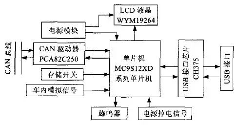
Figure 1. Overall System Structure
2. System Hardware Design
Based on the overall system structure, the hardware circuit mainly consists of the following major modules: main controller module, LCD module, CAN driver module, power supply module, and CH375 interface circuit module.
2.1 Main Controller Module
The system CPU uses Freescale’s MC9S12XD series microcontroller. It is the core of the control and communication parts, responsible for system initialization settings and message reception, as well as related data judgment processing and display. The chip integrates almost all analog and digital peripherals and other functional components required for the microcontroller control system and data acquisition system. Its main features are as follows:
(1) The MC9S12XD series comes with a unique XGATE coprocessor. In this system, the reception of CAN signals is handled by an interrupt routine, which is processed by the XGATE, thereby reducing the CPU load and improving system response speed.
(2) It has 16 analog-to-digital conversion channels, providing hardware support for collecting analog signals with programmable precision down to 10 bits.
(3) It features 5 MSCAN modules with an integrated CAN controller, making the configuration of the CAN module essentially a configuration of the corresponding registers of the microcontroller, which is convenient and flexible.
(4) Support for background debugging mode (BDM) makes debugging the chip extremely convenient, accelerating the product development cycle.
(5) A rich set of interrupt sources provides ample assurance for the system to operate without operating system support.
2.2 LCD Display Module
The system uses a WYM19264 LCD, displaying on 3 screens, each capable of showing a 64×64 dot matrix. The external interface of this LCD uses a 20-pin socket, and the connection circuit to the microcontroller is relatively simple. The chip select signals CS1 and CS2 are connected to microcontroller pins PH6 and PH5, respectively, while control signals RS, R/W, and EN are connected to PK4, PJ1, and PJ0, respectively. The 8 data lines (DB0~DB7) are connected to 8 pins of the PB port (PB0-PB7) for parallel transmission.
2.3 CAN Driver Module
The CAN driver interface chip selected is PAC82C250, which is designed for high-speed communication (up to 1Mbps) in automotive applications. This device provides differential transmission capability for the bus and differential reception capability for the CAN controller, protecting the bus from instantaneous interference in automotive environments. Pin 8 (Rs) allows for the selection of different operating modes: high-speed, standby, and slope control. In this system, pin 8 is grounded to select high-speed mode. RX and TX are connected to the microcontroller’s CAN module pins, specifically the CAN0 module, connected to RXCAN0 and TXCAN0.
2.4 Power Supply Module
The power supply for the logger is derived from the 12V vehicle battery. This power supply, in addition to powering the system, also provides power for ignition, lighting, signaling, and other devices. Due to significant power fluctuations and interference, the power supply module must be carefully designed to meet the demands, especially considering that the logger’s power interface may become loose or poorly connected due to severe vibrations while the vehicle is in motion.
The circuit diagram of the power supply module is shown in Figure 2, where U1 is the 6V backup power provided by the battery, and U2 (main power) is the vehicle’s 12V power supply. This power supply module is divided into two paths, with the +5V voltage from the 7805 voltage regulator supplying power to the LCD, while the VCC converted from the 4275 powers the microcontroller and auxiliary circuits. During normal operation, D1 is in the off state, and the backup battery is inactive. Once the main power supply is lost, D1 quickly turns on, and the backup power supply automatically activates to power the system.
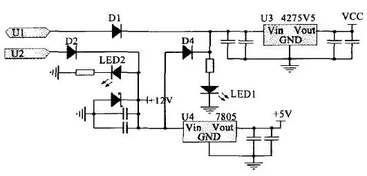
Figure 2. Power Supply Module
This design of the power supply module has two reasons, as follows:
(1) The use of a backup battery. The logger stores collected data by sequentially writing it into the clusters allocated for the recording file. When data collection ends, either due to the experimenter turning off the storage switch or power loss, the microcontroller must perform the important task of closing the recording file. Closing the file involves writing the actual length of the file and the total number of recorded data into the relevant header of the file. If the file is not correctly closed, or if power loss occurs before the file can be closed, Windows will be unable to find the end of the file, and the PC software will also fail to open the file, resulting in the loss of the collected data. To prevent data loss due to power failure, this system employs a backup battery.
(2) Separate power supply for the microcontroller and LCD. When the main power is functioning normally, the entire system is powered by the main supply. Once the main power fails, the backup battery only powers the microcontroller to complete the file closure process, while the LCD is powered down. Since the LCD consumes a significant amount of power and the backup battery has limited capacity, this separate power supply design not only meets the power needs for file closure but also conserves battery power.
Of course, the backup battery cannot be used for extended periods and is only intended for emergency file closure. Therefore, a power detection signal is designed. Once a power failure is detected, a buzzer and LED are activated to alert the user that the power supply is abnormal and requires inspection of the logger’s power connections.
2.5 CH375 Interface Circuit Module
The USB interface chip used in this system is CH375 from Nanjing Qinheng Electronics, which supports both host and device modes. It features an 8-bit data bus, read, write, chip select control lines, and interrupt output, allowing for easy connection to the microcontroller’s system bus. It also includes firmware that handles the communication protocol for mass storage devices, allowing the external microcontroller to read and write the USB drive directly in sector units.
The read select signal RD#, write select signal WR#, and chip select signal CS# are all input signals and are active low. CS# is the interrupt request output signal, also active low. The A0 signal is used to distinguish between commands and data; when A0=1, commands can be written, and when A0=0, data can be read or written. The 8-bit bidirectional data bus is connected to the microcontroller’s PA port (PA0-PA7) for parallel transmission. The hardware supports automatic detection of USB device connections. In host mode, when properly connected, the ACT# pin outputs a low level, allowing the ACT# I pin to be externally pulled up with a resistor and connected in series with an LED to indicate whether the USB device is functioning correctly.
When laying out the PCB, the 7805 chip should be placed at the edge of the board in a location with good heat dissipation, and away from the LCD screen. Testing has shown that the 7805 chip generates a significant amount of heat, and if used for long periods near the LCD screen, it can affect the display quality. Additionally, the power module’s LED should be placed close to the power interface, while the USB module’s LED should be situated near the USB module, with different colors to facilitate user observation.
3. System Software Design
The software design adopts a modular approach and interrupt calling scheme. Upon powering on the system, initialization is performed first. Information on the CAN bus is received via interrupts, with the interrupt routine processed by the XGATE. Each time a frame of information is received, an interrupt is generated to trigger the microprocessor to enter the interrupt service routine, where the frame data is read and temporarily stored in a buffer. This buffer is shared between the XGATE and the CPU. Since the data read from the USB drive is in sector units, this system sets the buffer size to one sector (512 bytes). When the buffer is full, the main program transfers the data to the USB drive.
The main functional modules of the system software include: main program module, initialization module, and interrupt handling module.
3.1 Main Program Design
The flowchart of the main program is shown in Figure 3.
As seen in flowchart 3, the entire program runs in a polling mode to detect whether the power supply has failed. Since the CAN signal packet frequency inside the vehicle is typically in the tens of milliseconds, if the LCD screen displays data in real-time, the screen refresh rate would be too fast for observation. Therefore, this system is designed to refresh the screen data once when the buffer is full, which is sufficient for user needs, regardless of whether the storage switch is closed; the LCD screen will continue to provide display services. Sudden power loss during recording or the user turning off the storage switch will result in the closure of the currently recorded file, modifying the file pointer and file length, along with other file system-related handling.
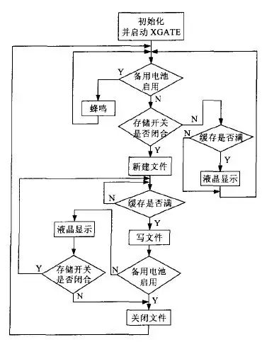
Figure 3. Main Program Flow
3.2 Initialization Module
(1) Initialization of the CAN Module
The initialization design of the CAN controller is crucial and must consider every register written carefully and comprehensively. If initialization fails, the system will not function correctly. This logger essentially acts as an additional node in the entire CAN network for communication, and all CAN nodes in the network must synchronize. To initialize the CAN module, it must first enter initialization mode. By setting the IN-ITRQ (CANCTLO) bit to initiate a request and receiving a response from INITAK (CANCTL1), the MSCAN enters initialization mode. In this mode, registers such as CAN-BTR0, CAN-BTR1, CAN-IDAR, and CAN-IDMR are typically configured. CAN-BTR0 determines the values for the baud rate prescaler and synchronization jump width, while CAN-BTR1 determines the width of the cycle, the position of the sample point, and the number of samples taken at each sample point, with appropriate values set based on the specific CAN bus communication rate. CAN-IDAR and CAN-IDMR together determine which ID frames need to be received. In this system, the purpose of the CAN bus logger is to receive all CAN line data messages, so CAN-IDMR is set to 0xFFh, meaning all bits are not masked, and all frames are received. Once the necessary registers are configured, it must exit initialization mode to participate in CAN bus communication.
(2) CH375 Initialization
This mainly involves setting the USB operating mode using the SETUSBMODE command provided by CH375. The mode code is set to 06H, which indicates the USB host mode, automatically detecting whether a USB device is connected. Interrupt notifications are generated for the external microcontroller when a USB device is connected or disconnected, and a USB frame start packet (SOF) is periodically sent to the connected USB device. Typically, setting the USB operating mode is completed within 20 microseconds, and the operation status is output afterward. The operation status is read from the PA port to check if the setup was successful. If it is not successful, it indicates an error with CH375, such as incorrect chip model, being in serial mode, or unsupported modes, which would prevent reading and writing to the USB drive.
3.3 Interrupt Handling Module
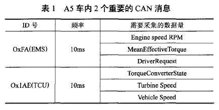
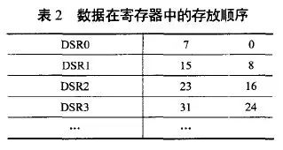
The interrupt module receives interrupts. Since this system is set to receive all frames, it is necessary to judge and “decode” the received frames in the interrupt handling function. The decoding process will be explained in detail using an example, as shown in Table 1, which lists two important CAN messages in the A5 vehicle, both using standard format (11 bits), with a data unit of 64 bits (8 bytes). After receiving the data frame in the interrupt, the ID number is first retrieved. For the standard frame format, IDRO stores IDIO~ID3, and the high 3 bits of IDR1 store ID2~ID0, thus the ID number can be calculated as (IDR0>5), setting the ID number as an int type variable. After obtaining the ID number, the message is decoded according to the message list. For example, if the obtained ID number is 0xFA, which is a message frame from the Engine Management System (EMS), we will extract the relevant data from its 64-bit data unit, with the storage order in the result registers DSR0-DSR7 as shown in Table 2. For the 16-bit Engine Speed RPM data, since the selected microcontroller uses Motorola big-endian mode, the least significant bit is in the 8th bit of DSR1, rather than the 0th bit of DSR0, and our upper-level PC data analysis software is in Intel format, necessitating byte order conversion for multi-byte data. Below is an example of function statements:
Engine Speed RPM DSR1;
Engine Speed RPM =(Engine Speed RPM<<8)|DSR0;
Mean Effective Torque=DSR2;
Driver Request=DSR3;
For multi-byte data, byte order conversion is required, while single-byte data can be copied directly. The collected data is stored in the buffer, and then the interrupt ends.
3.4 Other Modules
The LCD module uses “predefined screens” to reduce the communication load and repetitive tasks during operation for fixed display parts. The read/write USB module stores data on the USB drive in file format, and the microcontroller reads and writes to the USB drive primarily based on the FAT file system. The CH375 provides a library of USB file-level subroutines that support FAT16 and FAT32 file systems, allowing users to call various API functions from this library to read and write data blocks. The A/D conversion module requires careful configuration of control register 5 (ATDCTL5), as writing to this register will interrupt the current analog-to-digital conversion sequence and start a new conversion sequence. It is recommended that this register be configured after the first four control registers.
4 Conclusion
The developed CAN bus dashcam has been successfully applied in various road tests of the A5 vehicle, including 30,000 km and 50,000 km tests, accurately recording important data during driving. This provides crucial data for researchers for performance analysis, fault analysis, and calibration work. Using a CAN-based dashcam in vehicles equipped with a CAN bus significantly reduces system complexity and cost. For different vehicle models, only minor software modifications are needed without changing hardware, making the logger highly flexible and portable, thus widely applicable to various vehicle models.