1. Introduction
The design of the reset tree for SoC (System on Chip) is a critical aspect that ensures the chip can reliably start and recover under various conditions. The reset tree, as a crucial yet often overlooked infrastructure within the SoC, is responsible for safely, reliably, and orderly transmitting reset signals generated externally or internally to every logic unit that requires resetting, ensuring that the chip can operate from a defined initial state. The complexity of reset tree design is high, and verifying its ability to correctly reset in all operational modes is a significant challenge. Errors in reset design can lead to metastability, glitches, or other functional failures, potentially rendering the chip completely unusable. Therefore, a deep understanding and mastery of the core concepts, objectives, and key considerations of SoC reset tree design are essential for the design and verification of SoCs.
2. Concept of the Reset Tree
The reset tree can be likened to the root system of a tree, with the entire distributed network from the source to the terminal representing the reset tree.
Tree Roots: The source of the reset, such as external reset pins (POR_n, RESET_n), watchdog resets, software-triggered resets, etc.
Tree Trunk and Branches: The propagation path of the reset signal within the chip after synchronization, shaping, and distribution.
Tree Leaves: The various functional modules (such as CPU cores, DSPs, peripherals, memory controllers, etc.) that ultimately receive the reset signal.
3. Core Objectives of Reset Tree Design
1. Reliability: Ensure that the reset signal itself is glitch-free and can be captured stably to prevent metastability.
2. Controllability: Ability to independently control the reset of different parts of the chip (isolated reset). For example, resetting only one peripheral without affecting the CPU is crucial for debugging and low-power management.
3. Synchronization: Ensure that the release (de-assertion) of the reset signal is synchronized with the target clock domain, which is the most critical means to avoid metastability.
4. Orderliness: Control the sequence of reset and release from reset. Typically, the “reset release order” and “clock enable order” must follow certain rules to ensure logical correct initialization.
5. Testability: The design should support DFT (Design for Testability), such as scan chain testing, which usually requires a global reset to control the test mode.
4. Key Components and Design Points of the Reset Tree
1. Reset Sources
Power-On Reset (POR): The fundamental reset that occurs after the power stabilizes.
External Pin Reset: Triggered by users or external systems.
Watchdog Reset: Triggered by the watchdog timer after the system software runs amok.
Software Triggered Reset: Generated by writing to specific registers in software.
Low Power Mode Exit Reset: Requires resetting part of the logic when waking from certain deep sleep modes.
2. Reset Synchronizer
The reset synchronizer is the core technology of the reset tree, and asynchronous reset signals must never directly affect the reset pins of sequential logic.
Purpose: To synchronize asynchronous reset signals to the target clock domain, ensuring that no metastability occurs when the reset is released.
Classic Structure: Uses a two-stage or multi-stage D flip-flop chain (synchronizer) to “synchronize” the reset release signal.
3. Reset Controller
The reset controller is a centralized module that manages all reset sources and reset requests. Functions include aggregation, arbitration, distribution, and pulse generation.
Aggregation: Receives all internal and external reset requests.
Arbitration: Determines the priority of resets (e.g., power-on reset has the highest priority).
Distribution: Allocates the processed reset signals to different clock domains and power domains.
Pulse Generation: Ensures that the reset signal has sufficient pulse width (usually achieved through a counter).
4. Reset Distribution Network
Routes the synchronized reset signals throughout the chip.
Challenges: Reset signals typically form high fan-out networks, which can lead to significant clock skew.
Solutions: Clock tree synthesis: Treat the reset tree like a clock tree, using balanced buffer trees to reduce skew. Global network: Use dedicated global low-skew networks to transmit the main reset signal.
5. Domain Isolation Handling
Modern SoCs often have multiple clock domains and power domains, and the reset tree must handle cross-domain operations.
Clock Domain Crossing: Provide independent synchronizers for each clock domain. A reset signal needs to be synchronized to all clock domains it affects.
Power Domain Crossing: When a reset signal needs to be transmitted from a always-on domain to a power-gated domain, an isolator must be used. When the target domain is powered off, the isolator clamps the reset signal to a safe value (usually an invalid state) to prevent undefined levels from propagating to the always-on domain, causing leakage or latch-up effects.
6. Reset Sequence
Reset release sequence: Typically requires releasing the reset of basic units such as bus controllers, clock generators, and PLL locks first, followed by the reset of main control units like CPUs and DMAs, and finally the reset of peripherals. This sequence is usually precisely controlled by counters or state machines.
Relationship between reset and clock: Reset must be released after the clock is valid. Ideally, the clock should be running during the reset period.
5. Design Process and Verification
1. Architecture Definition
Define reset sources, reset types (synchronous/asynchronous, active high/active low), and reset domain partitioning.
2. RTL Implementation
Write RTL code for the reset controller, clearly using synchronous release structures.
3. Synthesis and Implementation
Tools will handle buffering and routing of high fan-out reset networks.
4. Verification
Simulation: Verify the behavior under various reset scenarios.
Static Verification: Use formal tools to check whether the reset signals can indeed reach all target registers (resetability check).
Timing Analysis: Confirm that the reset path meets timing requirements, especially the setup and hold times of the synchronizer itself.
6. Key Points in Reset Tree Design
1. Handling Mixed Reset Types
Resets are typically defined as asynchronous or synchronous relative to the clock. Sometimes, one reset signal may be used as a synchronous reset for one clock and an asynchronous reset for another clock, which requires special attention.
2. Reset Design for Registers
Allowing both asynchronous reset and set in registers is usually not a good idea, as this can lead to race conditions, resulting in mismatches between simulation and synthesis.
3. Verification of the Reset Tree
Traditionally, simulation has been the primary method for verifying reset behavior, but simulation test coverage is incomplete, and gate-level simulation is usually run late in the design cycle. Therefore, more advanced verification methods are needed to ensure the correctness of reset tree design.
7. Considerations in Reset Tree Design
1. Design of Power Domains and Voltage Sources
Design voltage domains based on different voltages and power domains based on different subsystem functions. This helps ensure the correct propagation of reset signals across different power domains.
2. Debouncing of Reset Signals
For reset sources like reset pins that may be affected by jitter, debouncing is necessary.
3. Design of Reset Delay Counters
During unstable clock phases, counters may become confused or sample incorrectly, leading to jumps in count values. Therefore, analog circuits should have a certain delay when generating POR, and the bit width of digital counters should be wide enough.
8. Future Trends in Reset Tree Design
As the complexity of SoC design continues to increase, reset tree design must also adapt to new challenges. For example, for SoCs with multiple clock domains and power domains, reset tree design needs to be more flexible and reliable. At the same time, with the development of hardware design verification technologies, the verification methods for reset trees will also become more advanced and efficient.
9. Case Study of Reset Solutions
No suitable examples were found, only a configuration scheme for external reset circuits of SoCs was located.
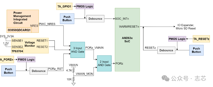
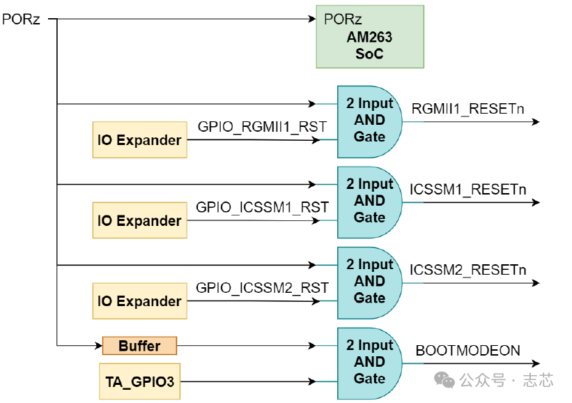
In TI’s AMZ63x SoC, the PORz signal is the power-on reset signal for the main domain, driven by a 3-input AND gate. When the PMC drives NRES, the MCU reset output signal is low, or the voltage monitor drives RESET1 or RESET2, or the user presses button SW2, or the test automation head outputs a low signal TA_PORZn, the power-on reset for the main domain is generated. The PORz signal connects to multiple modules, such as the PORz input of the AMZ63x SoC, RGMII Ethernet PHY reset, etc. Additionally, WARMRESETn is the warm reset signal.
10. Conclusion
The design of the reset tree for SoCs is a complex and critical task that requires comprehensive consideration of various factors to ensure that the chip can reliably reset and start under all conditions. A well-designed reset tree is the cornerstone of stable SoC operation.
Join the community
dsfsdfsdf

As of 20250903, the article contains a total of 196,188 words, with 169 documents (manuals).
LSF: 1 document (manual)
VIM Editor: 1 document (manual)
MakeFile: 1 document (manual)
RTL Code: 5 documents (manual)
SoC Design: 9 documents (manual)
SoC Clock: 1 document (manual), article 1874 words.
SoC Reset: article 2663 words.
SRAM Design: 1 document (manual)
ARM Architecture: 5 documents (manual), article 18810 words
Chip Manufacturing: 1 document (manual)
Research Reports: 7 documents
SPICE Netlist: 3 documents (manual)
Physical IP: 4 documents (manual)
Physical File Formats (def, lef, etc.): 1 document (manual)
Work Insights: 1867 words
Timing Libraries: 4 documents (manual)
Conformal ECO: 6 documents (manual)
Chip Testing: article 3826 words
Crosstalk Noise: 1 document (manual), article 2000 words
3D IC: 1 document (manual), article 1383 words
Scripts: 10 documents (manual), article 12524 words
DFT: 21 documents (manual), article 38963 words
Low Power Design: 20 documents (manual), article 7449 words
Timing Analysis (Constraints): 23 documents (manual), article 58015 words
Formal Verification: 3 documents (manual), article 2325 words
Power (Voltage Drop) Analysis: 7 documents (manual), article 10897 words
Physical Verification: 6 documents (manual), article 2334 words
Logic Synthesis: 6 documents (manual), article 5462 words
Layout and Routing: 9 documents (manual), article 9562 words
Hierarchical Layout and Routing: 1 document
Low Power Design Layout and Routing: 5 documents
Clock Tree: 5 documents (manual), article 10103 words
Process Library: 1 document (manual), 5662 words
Domestic EDA: 3 documents
Tweaker ECO: 1 manual
DRC Marker Usage: 1 manual
Chip Testing: 1 document (manual)
Post-Simulation: 1 document (manual)
Community Highlights: Regular updates.
Industry Research Community: Various industry research reports will be shared regularly.
dsfsdfsdf