Introduction
The field of artificial intelligence is rapidly evolving, with on-chip AI capabilities shifting from traditional Convolutional Neural Networks (CNNs) to transformer-based generative AI models. This article explores the cutting-edge Neural Processing Unit (NPU) implemented in the Samsung 4nm Exynos 2400 System on Chip (SoC), designed to meet the stringent requirements of both traditional and generative AI workloads [1].
1
Challenges of Generative AI Models
Generative AI models, such as large language models (LLMs, e.g., LLaMA) and large visual models (LVMs, e.g., Stable Diffusion), present unique computational challenges compared to traditional neural networks. LLMs require reading several gigabytes of weight data from DRAM during each token generation process, making them memory-intensive. In contrast, LVMs are more compute-intensive but exhibit distinct computational characteristics, where softmax and layer normalization operations account for approximately 40% of the total computation time.
This is significantly different from CNNs, where convolution operations typically constitute 90-99% of the computational workload. These new requirements necessitate a rethinking of NPU architecture to efficiently support the diverse operations required by generative AI models.
2
Heterogeneous NPU Architecture
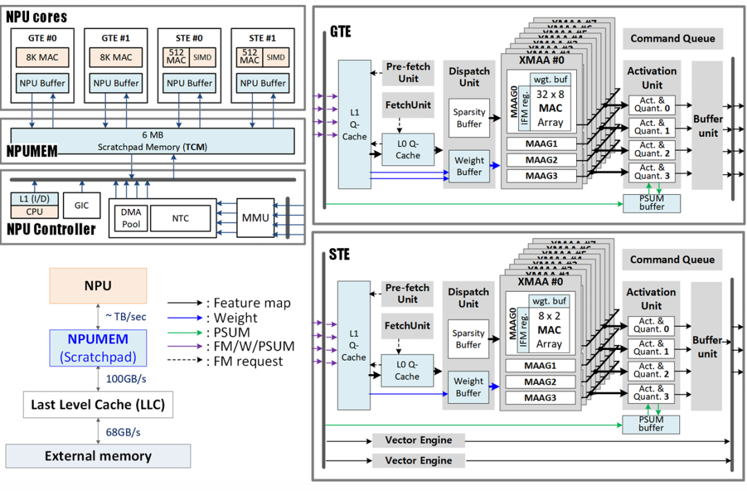
Figure 1: Heterogeneous architecture of the Neural Processing Unit, showcasing various tensor engines, vector engines, and memory hierarchy.
The NPU architecture presented in this article adopts a heterogeneous approach to meet the diverse computational needs of different neural network operations. As shown in Figure 1, the NPU integrates two types of tensor engines (TEs) and vector engines (VEs), each optimized for specific types of operations.
The General Tensor Engines (GTEs) consist of 8K MAC (Multiply-Accumulate) units optimized for compute-intensive operations such as convolution and matrix-matrix multiplication. Shallow Tensor Engines (STEs), each containing 512 MACs, are designed to handle memory-intensive operations more efficiently, such as matrix-vector multiplication and depthwise separable convolutions.
Complementing these tensor engines are four vector engines (VEs), which utilize Single Instruction Multiple Data (SIMD) data paths and 32 execution units. These VEs are specifically designed to handle nonlinear operations, such as softmax, complex activation functions, and normalization operations, which are common in transformer-based models.
All these processing engines are connected to a 6MB shared scratchpad memory, referred to as NPUMEM, used for storing input and output feature maps, intermediate data, and weight values. This shared memory architecture facilitates efficient data sharing between different processing engines.
3
Optimized Memory Hierarchy with Queue Caches
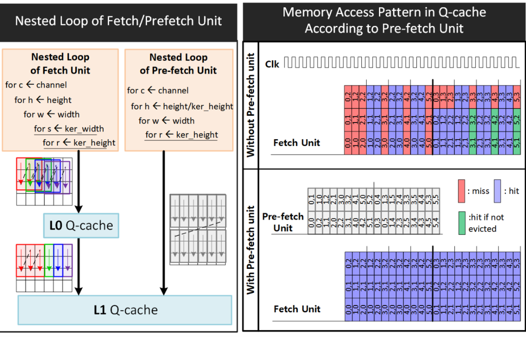
Figure 2: L0/L1 queue cache operations, illustrating how data sequences are managed to optimize locality and reduce memory access latency.
A key innovation of this NPU design is the implementation of L0/L1 queue caches (Q-cache) within each tensor engine. Unlike traditional caches, these Q-caches are designed to reduce miss penalties by leveraging the predetermined order of operations within the tensor engines.
As shown in Figure 2, the Q-cache manages data sequences as queues, intuitively understanding the temporal and spatial locality of incoming data requests. This allows for more precise eviction decisions, significantly improving cache hit rates after initial cold misses. Additionally, the prefetching capability directly loads data into the L1 Q-cache, minimizing initial cold misses and further reducing latency.
This approach effectively hides latency without the need for complex scheduling or task management techniques, such as Single Instruction Multiple Threads (SIMT). For CNN operations, the prefetch unit can operate several cycles ahead of the fetch unit, significantly improving L1 Q-cache hit rates and enhancing overall performance.
4
Skew-Based Tile Partitioning for Data Reuse Optimization
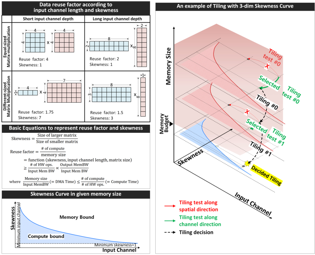
Figure 3: Tile selection method using skew curves, demonstrating how matrix size, shape, and input channel length affect data reuse efficiency.
This article introduces an innovative method for optimizing data reuse within the memory hierarchy based on matrix characteristics. As shown in Figure 3, three key factors influence data reusability: matrix size, the relative size of feature maps and weight matrices (defined as skew), and input channel length.
Higher data reuse rates can be achieved when larger matrices are stored in memory, when feature maps and weight matrices are of similar sizes, and when matrices have shorter input channel lengths. Skew is defined as the ratio between larger and smaller matrices, while the minimum reuse factor indicates the minimum amount of data reuse required to bridge the bandwidth gap between input and output ports within the memory hierarchy.
The skew curve in Figure 3 illustrates the relationship between skew and input channel length for a given memory size. This curve helps determine whether a specific tile configuration is compute-intensive (blue area) or memory-intensive. By extending this concept to three dimensions to accommodate various memory sizes, the NPU can efficiently perform matrix/tensor tile partitioning within the available memory budget, maximizing data reuse.
The tile partitioning process uses a heuristic method based on the skew curve. Starting with tiles larger than the memory budget, the system greedily selects the tile partitioning direction (width, height, or input channel) referencing the skew curve. After each tile partitioning step, the skew curve is updated to match the new tile size. This process continues until the tile size fits within the memory budget, ensuring optimal data reuse throughout the computation process.
5
Parallel Processing with Heterogeneous Engines
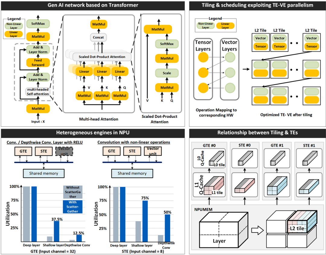
Figure 4: Neural network operations using heterogeneous engines, illustrating how TEs and VEs collaborate for parallel processing of different operations at the tile level.
In transformer-based networks, linear operations alternate with nonlinear operations (such as softmax), which account for a significant portion of the overall computation. To reduce computation latency, the NPU enables tensor engines (TEs) and vector engines (VEs) to execute in parallel.
As shown in Figure 4, the entire neural network is partitioned into large L2 tiles, sized appropriately for processing in NPUMEM at once, considering the parallel processing capabilities of TEs and VEs. These L2 tiles are further divided into smaller L1 tiles, taking into account the L1 Q-cache of the tensor engines. Each TE processes one L1 tile at a time, continuously until all computations for the L2 tile are completed.
The NPU implements tile-level pipelining, with TEs and VEs exchanging input and output tiles with NPUMEM. Multiple TEs can also execute in parallel, leveraging tile-level parallelism to accelerate the computation of L2 tiles. This collaborative approach ensures efficient processing of both linear and nonlinear operations.
While General Tensor Engines (GTEs) are optimized for convolution and matrix-matrix multiplication with high data reuse, they may achieve lower hardware utilization for memory-intensive operations such as matrix-vector multiplication or depthwise separable convolutions. Shallow Tensor Engines (STEs), although having fewer MACs, compensate for this limitation by achieving higher hardware utilization through higher memory bandwidth per MAC in these operations. This heterogeneous architecture provides functional flexibility to efficiently handle various types of neural network layers.
6
Thermal Management and Packaging Innovations
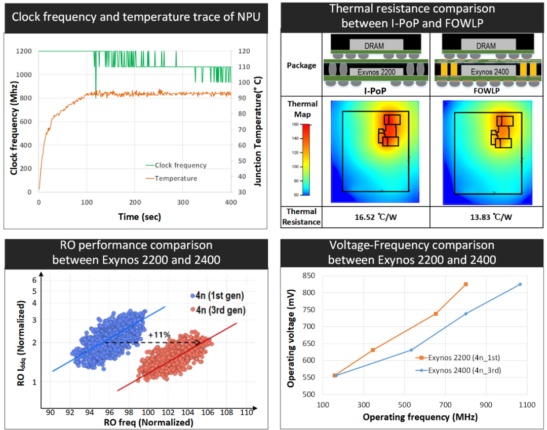
Figure 5: NPU performance improvements achieved through RO AC performance gains and reduced thermal resistance, demonstrating how process and packaging innovations enhance clock frequency at the same power level.
The high density of MAC units within a small silicon area can lead to thermal management challenges. As shown in Figure 5, NPU performance is thermally limited, necessitating a reduction in clock frequency to prevent excessive junction temperatures.
To overcome these thermally induced performance limitations, the NPU employs two key innovations. First, it utilizes an enhanced third-generation 4nm process, providing an 11% gain in ring oscillator (RO) AC performance compared to the first-generation 4nm process. This improvement is achieved through source and drain engineering, reduced interlayer line resistance, and optimized alternative metal gates, lowering effective capacitance and resistance.
Second, the NPU adopts a fan-out wafer-level packaging (FOWLP) solution with excellent thermal characteristics. Compared to the interconnect layer packaging stack (I-PoP) used in the previous Exynos 2200, the FOWLP in the Exynos 2400 offers better thermal resistance characteristics. The larger chip thickness and thinner redistribution layer in FOWLP enhance heat dissipation, reducing thermal resistance from 16.52°C/W to 13.83°C/W, a decrease of 16%.
The combined effects of process improvements and packaging innovations have increased the maximum clock frequency of the NPU by 30% at the same power level, significantly enhancing the overall performance of AI applications.
7
Performance Results and Conclusion
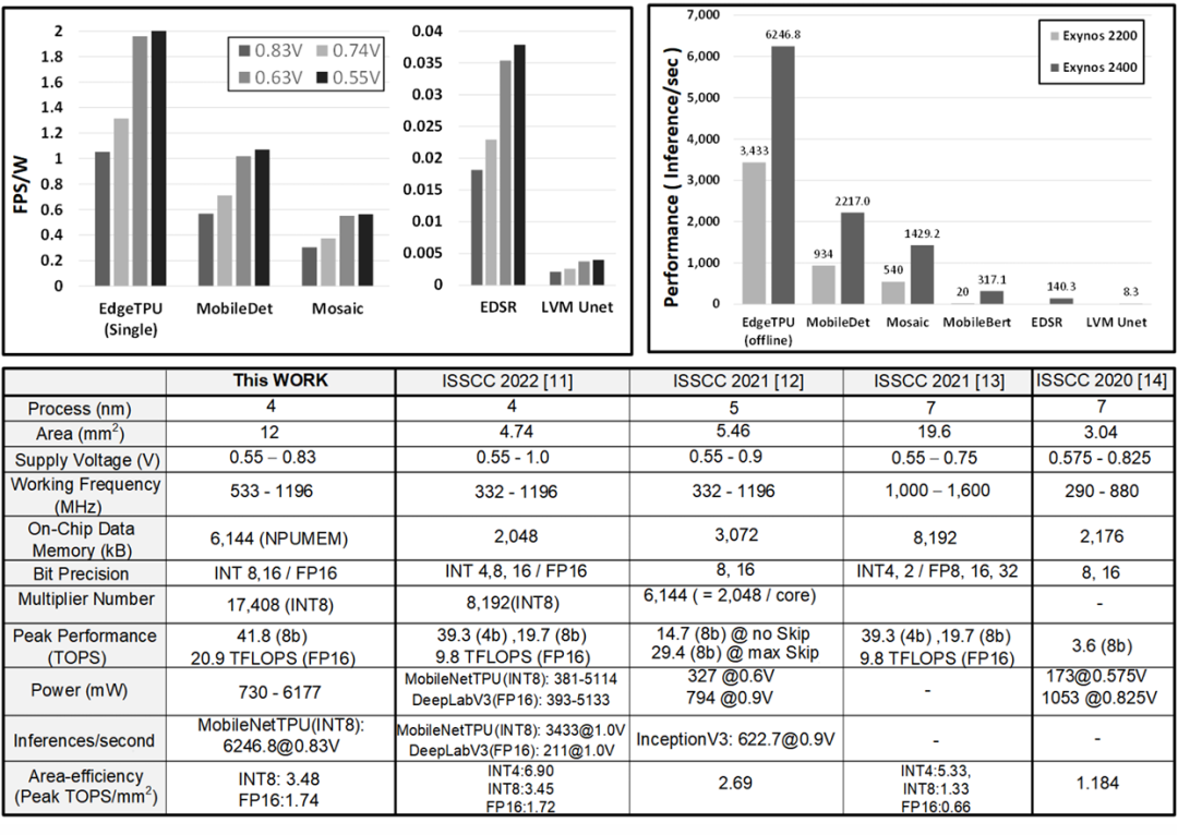
Figure 6: Measurement results and performance comparison table, showcasing the specifications and performance metrics of the NPU across various neural network benchmarks.
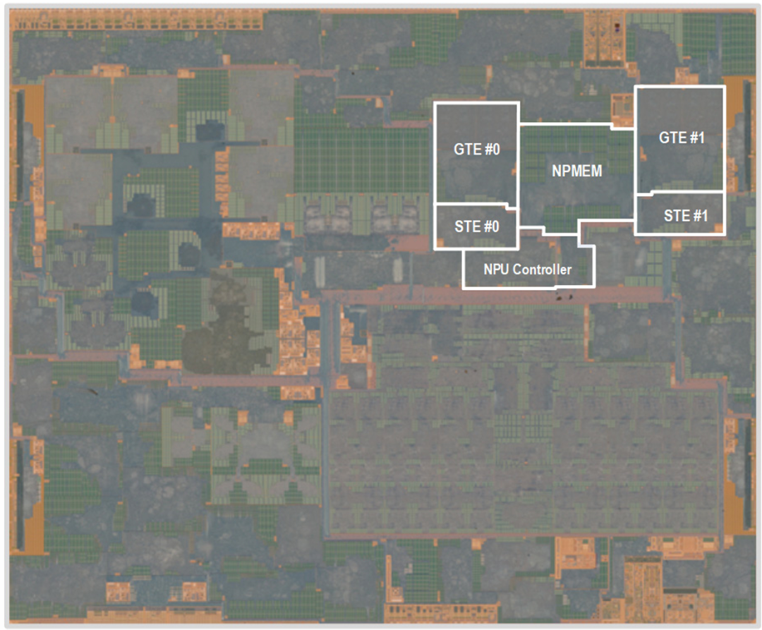
Figure 7: Microscopic photo of the Exynos 2400 SoC chip, highlighting the NPU area within the chip.
The NPU occupies a silicon area of 12 square millimeters, operating at a voltage range of 0.55V to 0.83V, with a clock frequency range from 533MHz to 1196MHz. As shown in Figure 6, the NPU demonstrates impressive performance across various neural network benchmarks.
Compared to previous implementations, the inference throughput for MobileNetEdgeTPU, MobileDet, and Mosaic networks has increased by 1.81x, 2.37x, and 2.65x, respectively, at 1196MHz. Additionally, the NPU achieves 140.3 inferences per second on EDSR and 8.3 inferences per second on the U-net network used in Stable Diffusion (LVM).
Despite the increase in internal buffer size from 2MB to 6MB, the NPU maintains an area efficiency of 3.48 TOPS/square millimeter due to optimized MAC design and spatially shared weight buffers across MACs. Figure 16.3.7 shows a microscopic photo of the Exynos 2400 SoC chip highlighting the NPU.
This innovative NPU architecture represents a significant advancement in on-chip AI capabilities, efficiently supporting both traditional CNN-based applications and emerging transformer-based generative AI models. By combining heterogeneous processing engines, optimized memory hierarchy, intelligent tile partitioning strategies, and advanced thermal management solutions, the NPU delivers the performance required for next-generation mobile AI applications while maintaining power efficiency.
References
[1] A. Vaswani, et al., “Attention Is All You Need”, NeurIPS, 2017.
[2] A. Dubey, et al., “The Llama3 Herd of Models”, ArXiv, 2024.
[3] R. Rombach, et al., “High-resolution image synthesis with latent diffusion models”, ArXiv, 2021.
[4] J.R. Stevens, et al., “Softermax: Hardware/Software Co-Design of an Efficient Softmax for Transformers”, DAC, 2021.
[5] B. Klenk, et al., “Relaxations for High-Performance Message Passing on Massively Parallel SIMT Processors”, Int. Parallel and Distributed Processing, 2017.
[6] T. Yoo, et al., “Advanced Chip Last Process Integration for Fan Out WLP”, IEEE ECTC, 2022.
[7] V.J. Reddi, et al., “MLPerf Inference benchmark”, ISCA, 2020.
[8] M. Tan, et al., “EfficientNet: Rethinking Model Scaling for Convolutional Neural Networks”, ICML, 2019.
[9] Y. Xiong, et al., “MobileDets: Searching for Object Detection Architectures for Mobile Accelerators”, CVPR, 2021.
[10] W. Wang, et al., “MOSAIC: Mobile Segmentation via decoding Aggregated Information and encoded Context”, ArXiv, 2021.
[11] J.-S. Park, et al., “A Multi-Mode 8k-MAC HW-Utilization Aware Neural Processing Unit with a Unified Multi-Precision Datapath in 4nm Flagship Mobile SoC”, ISSCC, pp. 246 247, Feb. 2022.
[12] B. Lim, et al,. “Enhanced Deep Residual Networks for Single Image Super-Resolution”, CVPR, 2017.
[13] J.-S. Park, et al., “A 6K-MAC feature-map-sparsity-aware neural processing unit in 5nm flagship mobile SoC”, ISSCC, pp. 152-153, 2021.
[14] A. Agrawal, et al., “7nm 4-Core AI Chip with 25.6TFLOPS Hybrid FP8 Training, 102.4TOPS INT4 Inference and Workload-Aware Throttling”, ISSCC, pp. 144-145, 2020.
[15] C.-H. Lin, et al., “A 3.4-to-13.3TOPS/W 3.6TOPS Dual-Core Deep-Learning Accelerator for Versatile AI Applications in 7nm 5G Smartphone SoC”, ISSCC, pp. 134-135, 2020.
END

The SEMICON event that just concluded at the end of March saw the launch of over 20 devices by New Kai, targeting these devices. The technical analysis between New Kai and its competitors has been deleted from this public account. For details, you can join the knowledge circle to see the original text.
At the end of February, I wrote about the actual situation of HH’s advanced process expansion and acquisition in the knowledge circle, and another calculation of the shipments of 910C this year. If interested, feel free to scan the QR code below to join the knowledge circle.
In early March, the hot topics were Hong Kong stocks such as Xiaomi, Alibaba, Tencent, and Kingsoft Cloud, which truly represent the solid targets of Chinese AI. The hardware representative Xiaomi, which has already tripled, why can it still maintain its strength? We will also explain in detail the future business development and performance growth data of Xiaomi.
If you are interested, you can directly scan the following QR code to join the knowledge circle. If you are not satisfied with the content, you can apply for a refund within three days. With over three thousand paid community members, you are welcome to join.