“This article details the process of hardware disassembly, firmware extraction, debugging, and modification of the Xbox One controller. The author explores the internal structure by disassembling the controller, identifies the SWD interface, and uses the OpenOCD tool for hardware debugging. The article also explains how SWD works, how to use OpenOCD for firmware extraction and modification, and how to perform real-time debugging of the controller using GDB. Ultimately, the author successfully modifies the firmware and verifies the modification results. ”

Objective When evaluating embedded platforms, there are many things you can do or try to accomplish. Through this article, I aim to demonstrate/test the following:
-
Can firmware be extracted from the target?
-
Is it possible to debug or probe the target in some way to gain a better understanding of its internal operations?
-
Can the firmware be modified or changed through software development or hardware modifications?
The first step in answering these questions is to disassemble the hardware.
Hardware Disassembly
After opening the casing, the following PCB is visible:
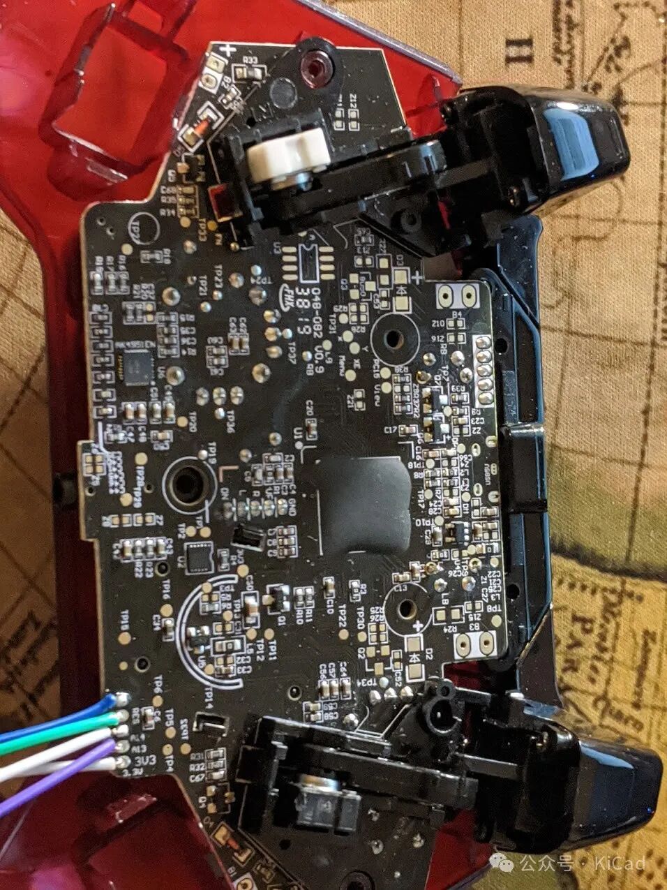
There isn’t much to see here as the main chip is covered in epoxy. Fortunately, many test pads are labeled, but the labeled pads seem to be test points for various button presses, so there’s nothing exciting.
At the bottom of the circuit board, there is an IC labeled AK4961, which is an audio codec chip. This chip is a low-power 24-bit stereo codec with microphone, headphone, and speaker amplifiers.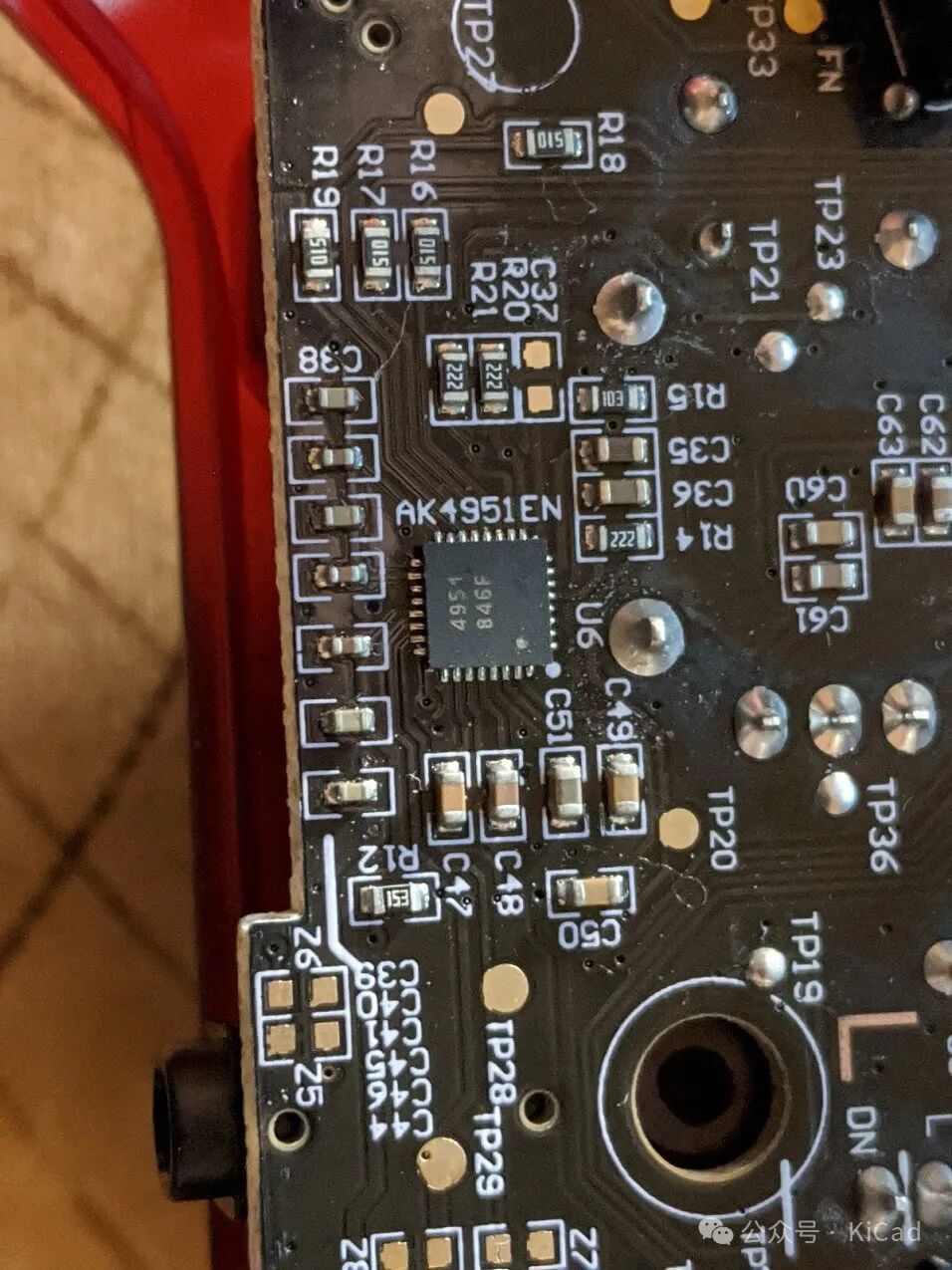
However, if we look to its right, we find a small group of pads withsome silkscreen labels:
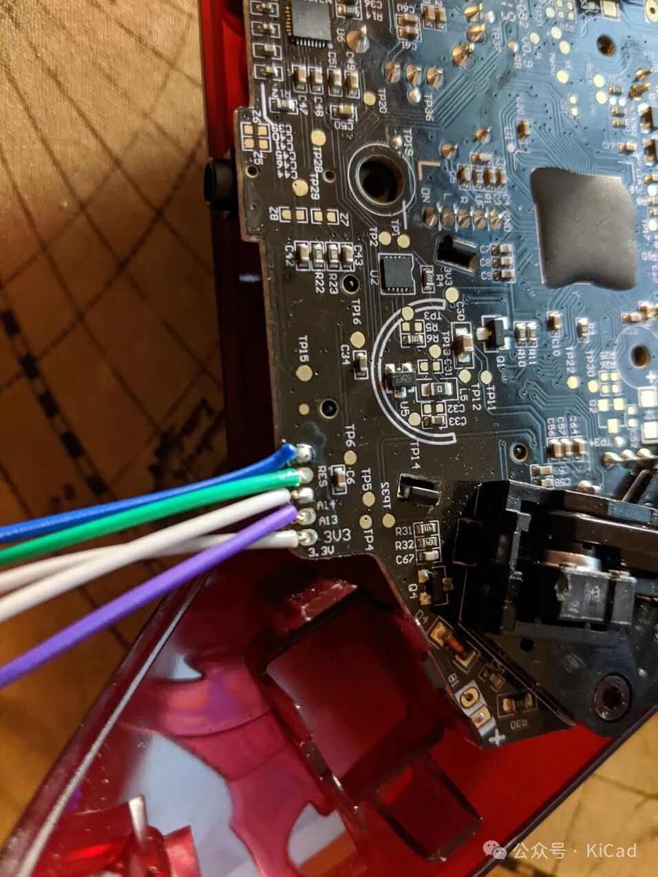
From the silkscreen, we can see labels for<span>3V3</span>, <span>A13</span>, <span>A14</span>, <span>RES</span>. We first measure the voltage on each pin with a multimeter:
| Pin | Value |
|---|---|
| 0/NA | 0 (ground) |
| RES | 3.3V |
| A14 | 0.1V |
| A13 | 3.3V |
| 3V3 | 3.3V |
RES, A14, or A13 show no fluctuations or modulation, so these must be for other purposes, but what? Given that one of the labels is<span>RES</span> (possibly representing system reset), it is very likely that there is a JTAG or SWD header present.
We can test if the RES pin actually resets the target by pulling it low with a 10k resistor (remember, we are reverse engineering here and do not want to accidentally short anything!). If you are not familiar with how these types of pins or system reset pins typically work — they are usually active low, meaning they are idle at a high level and must be pulled low to activate. So, if we monitor the output of dmesg -w and pull that line low with a 10k resistor, what do we see?
[ 2108.588884] usb 1-6.4: new full-speed USB device number 10 using xhci_hcd[ 2108.691108] usb 1-6.4: New USB device found, idVendor=0e6f, idProduct=02a2, bcdDevice= 1.0f[ 2108.691113] usb 1-6.4: New USB device strings: Mfr=1, Product=2, SerialNumber=3[ 2108.691116] usb 1-6.4: Product: PDP Wired Controller for Xbox One - Crimson Red[ 2108.691119] usb 1-6.4: Manufacturer: Performance Designed Products[ 2108.691122] usb 1-6.4: SerialNumber: 0000AE38D7650465[ 2108.698675] input: Generic X-Box pad as /devices/pci0000:00/0000:00:14.0/usb1/1-6/1-6.4/1-6.4:1.0/input/input25[ 2131.403862] usb 1-6.4: USB disconnect, device number 10[ 2133.420350] usb 1-6.4: new full-speed USB device number 11 using xhci_hcd[ 2133.522469] usb 1-6.4: New USB device found, idVendor=0e6f, idProduct=02a2, bcdDevice= 1.0f[ 2133.522474] usb 1-6.4: New USB device strings: Mfr=1, Product=2, SerialNumber=3[ 2133.522478] usb 1-6.4: Product: PDP Wired Controller for Xbox One - Crimson Red[ 2133.522480] usb 1-6.4: Manufacturer: Performance Designed Products[ 2133.522483] usb 1-6.4: SerialNumber: 0000AE38D7650465[ 2133.530103] input: Generic X-Box pad as /devices/pci0000:00/0000:00:14.0/usb1/1-6/1-6.4/1-6.4:1.0/input/input26Great, this caused the controller to reset, so we have eliminated one pin, leaving us with two pins.
When seeing a debug header like this, a common assumption is that it is for JTAG or some other form of hardware-level debugging. However, the JTAG specification requires at least 4 pins: TDO, TDI, TMS, and TCK. Our target only has two, so it is very likely this is a Serial Wire Debug (SWD) port.
Understanding SWD
SWD is a commonly used debugging interface for ARM Cortex targets. As the name suggests, SWD only requires one data line and one clock line, but how do we determine which is which? Before that, we should first understand how SWD works and what tools can be used to connect to SWD.
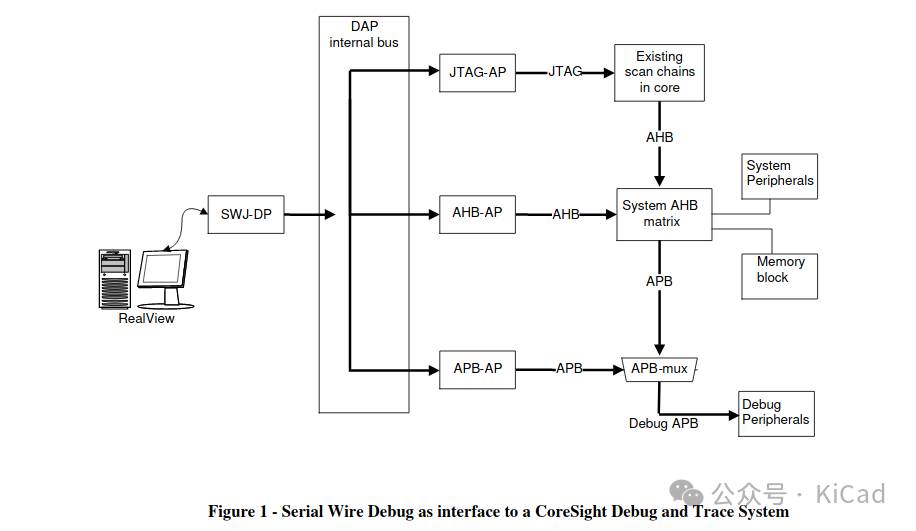
First, SWD connects to an interface called the “Debug Access Port” (DAP). The DAP provides access to various “Access Ports” (APs), which offer functionalities including typical hardware debugging, traditional JTAG cores, and other high-performance memory buses. The diagram below visually illustrates the architecture of DAP and AP.
Each AP consists of 64 32-bit registers, one of which is used to identify the type of AP. The functionality and features of the AP determine how to access and use these registers. You can find all relevant information about some standard APs here. The ARM interface specification defines two types of APs by default, namely JTAG-AP and MEM-AP. The MEM-AP also includes a discovery mechanism for discovering components connected to it.
SWD Protocol
As mentioned earlier, SWD was developed as a pseudo-alternative to JTAG. With SWD, the number of pins is reduced from 4 to 2 while providing a lot of the same functionality as JTAG. However, one downside of SWD is that devices cannot be chained together, whereas JTAG allows for that. Below are the two pins used in SWD:
| Pin | Usage |
|---|---|
SWCLK |
Clock signal sent to the CPU, determining when to sample and send data |
SWDIO |
Bidirectional data pin used for data transfer between the target CPU |
SWD utilizes a packet-based protocol to read and write registers in the DAP/AP, which includes the following phases:
-
Host to target packet request
-
Bus turnaround
-
Target host acknowledgment response
-
Data transfer phase
The packet structure is shown in the diagram below, and I have also listed the various fields in the table.
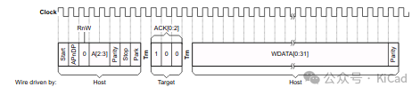
| Field | Usage |
|---|---|
| Start | Start bit, value 1 |
| APnDP | This bit indicates whether to access registers via the debug port or access port. |
| RnW | Read/Write bit |
| A[2:3] | Address field for AP or DP address |
| Parity | Parity bit for all packet requests |
| Stop | Stop bit (always 0) |
| Park | Line driven high during turnaround |
| ACK[0:2] | Target sends acknowledgment bits to the host |
| DATA[0:32] | Actual data frame, read from or written to the target based on the RnW bit |
| Parity | Final parity bit of the data frame |
After the Park bit (from host to target), there is a turnaround period, which essentially means the target will respond on the same line.
At a high level, the SWD port uses these packets with the DAP interface, which in turn allows access to the MEM-AP, providing debugging and memory read/write capabilities. In this article, we will use a tool called OpenOCD to perform these transactions. Next, we will review how to build and use OpenOCD.
OpenOCD
Install dependencies:
sudo apt-get install build-essential libusb-1.0-0-dev automake libtool gdb-multiarchClone the repository, configure, and build!
wrongbaud@115201:~/blog$ git clone https://git.code.sf.net/p/openocd/code openocd-codecd openocd-code./bootstrap./configuremake -j$(nproc)Once OpenOCD is built, we can attempt to debug the controller via SWD. To do this, we need to tell OpenOCD at least two things:
-
What we are using for debugging (which debug adapter we are using)
-
What target we are debugging
For debugging, we will use the FT2232H to dump the SPI flash. With this interface, we can use OpenOCD to query information from the target machine via SWD, which is crucial because at this stage of the reverse engineering process, we do not even know what the target CPU is!
Below is a table to determine which pins on the FT2232H need to be connected to the SWD target:
| FT2232H Pin | SWD Target |
|---|---|
AD1 |
SWD |
AD0 |
SCLK |
AD4 |
SRST (system reset) |
Finally, to use the FT2232H as an SWD adapter, a 470 OHM resistor must be added between the AD1/AD2 pins of the FT2232H.
After connecting the pins on the FT2232H to the target, we can use the following script to query the DPIDR register on the DAP controller:
# We are using an FT2232H so specify this hereinterface ftdi# Provide the VID/PID of the FT2232Hftdi_vid_pid 0x0403 0x6010# There are two channels, this is the defaultftdi_channel 0# To the best of my knowledge, this is used to properly set and configure the state of the lines we are usingftdi_layout_init 0x0018 0x05fb# Enable SWD for the lines that we are using, and the portftdi_layout_signal SWD_EN -data 0# This is used to specify the sRST pin, in our case we're using ftdi_layout_signal nSRST -data 0x0010# Here we are selecting SWD as opposed to another transport layer such as JTAGtransport select swd# Set the speed of the adapter, this will vary based on what your hardware supportsadapter_khz 100# Create a new dap, (TAP for JTAG terms) with name chip and role CPU, -enable lets OpenOCD to know to add it to the scanswd new dap chip cpu -enable# Create the DAP instance, this must be explicitly created according to the OpenOCD docs dap create chip.dap -chain-position chip.cpuAs shown, we can run this script with OpenOCD, and the output is as follows (note that there was no output the first time it was run, and after swapping the SWD/SCLK lines, the following output was printed). For the connection between the FT2232 and the controller, see the table below:
| FT2232H Pin | Controller |
|---|---|
AD1 |
SWD ( A13) |
AD0 |
SCLK ( A14) |
AD4 |
SRST (RES) |
wrongbaud@wubuntu:~/blog/stm32-xbox$ sudo openocd -f openocd.cfg Open On-Chip Debugger 0.10.0+dev-01040-ge7e681ac (2020-01-27-18:55)Licensed under GNU GPL v2For bug reports, read http://openocd.org/doc/doxygen/bugs.htmlInfo : FTDI SWD mode enabledInfo : Listening on port 6666 for tcl connectionsInfo : Listening on port 4444 for telnet connectionsInfo : clock speed 100 kHzInfo : SWD DPIDR 0x2ba01477Warn : gdb services need one or more targets definedGreat! We found a chip ID 0x2ba01477, and if we Google this ID, we will see many search results about various Cortex M / STM32 devices — this makes sense as this processor series supports SWD. Now we can communicate with the DAP, and we should see if we can determine the exact processor being used — if there is a configuration file written for that processor, we can dump the flash library and obtain additional auxiliary information from the target processor. With this extra information, we can tell OpenOCD to create a target using the Cortex M definition, allowing us to take full advantage of the DAP while trying to determine the target CPU and gain some more general functionality:
# Set up the GDB target for the CPU, cortex_m is the CPU type, target create chip.cpu cortex_m -dap chip.dap# init reads out all of the necessary information from the DAP, kicks off the debugging session, etcinit# Read out the information from the DAP, including the ROM table dap infoWhen we run OpenOCD with this configuration file, we see the following results:
wrongbaud@wubuntu:~/blog/stm32-xbox$ sudo openocd -f openocd.cfg Open On-Chip Debugger 0.10.0+dev-01040-ge7e681ac (2020-01-27-18:55)Licensed under GNU GPL v2For bug reports, read http://openocd.org/doc/doxygen/bugs.htmlInfo : FTDI SWD mode enabledInfo : clock speed 100 kHzInfo : SWD DPIDR 0x2ba01477Info : chip.cpu: hardware has 6 breakpoints, 4 watchpointsInfo : chip.cpu: external reset detectedInfo : Listening on port 3333 for gdb connectionsAP ID register 0x24770011 Type is MEM-AP AHB3MEM-AP BASE 0xe00ff003 Valid ROM table present Component base address 0xe00ff000 Peripheral ID 0x00000a0411 Designer is 0x0a0, STMicroelectronics Part is 0x411, Unrecognized Component class is 0x1, ROM table MEMTYPE system memory present on bus ROMTABLE[0x0] = 0xfff0f003 Component base address 0xe000e000 Peripheral ID 0x04000bb00c Designer is 0x4bb, ARM Ltd. Part is 0xc, Cortex-M4 SCS (System Control Space) Component class is 0xe, Generic IP component ROMTABLE[0x4] = 0xfff02003 Component base address 0xe0001000 Peripheral ID 0x04003bb002 Designer is 0x4bb, ARM Ltd. Part is 0x2, Cortex-M3 DWT (Data Watchpoint and Trace) Component class is 0xe, Generic IP component ROMTABLE[0x8] = 0xfff03003 Component base address 0xe0002000 Peripheral ID 0x04002bb003 Designer is 0x4bb, ARM Ltd. Part is 0x3, Cortex-M3 FPB (Flash Patch and Breakpoint) Component class is 0xe, Generic IP component ROMTABLE[0xc] = 0xfff01003 Component base address 0xe0000000 Peripheral ID 0x04003bb001 Designer is 0x4bb, ARM Ltd. Part is 0x1, Cortex-M3 ITM (Instrumentation Trace Module) Component class is 0xe, Generic IP component ROMTABLE[0x10] = 0xfff41003 Component base address 0xe0040000 Peripheral ID 0x04000bb9a1 Designer is 0x4bb, ARM Ltd. Part is 0x9a1, Cortex-M4 TPIU (Trace Port Interface Unit) Component class is 0x9, CoreSight component Type is 0x11, Trace Sink, Port ROMTABLE[0x14] = 0xfff42003 Component base address 0xe0041000 Peripheral ID 0x04000bb925 Designer is 0x4bb, ARM Ltd. Part is 0x925, Cortex-M4 ETM (Embedded Trace) Component class is 0x9, CoreSight component Type is 0x13, Trace Source, Processor ROMTABLE[0x18] = 0x0 End of ROM tableInfo : Listening on port 6666 for tcl connectionsInfo : Listening on port 4444 for telnet connectionsWith these new changes, we can not only interact with the DAP and MEM-AP, but we can also debug the target machine via GDB. We can also determine that the target CPU is from the STM32F2X series based on the 0x411 Part Number in the MEM-AP entry:
|
However, for fun, if we cannot access the DAP and want to determine what our target is through memory read/write, there are some common memory areas in STM32 CPUs used to store ID and flash information. With this information, we can modify the OpenOCD script to read these areas and look for relevant ID information! The table below lists the offsets needed for ID information:
| STM Series | Offset |
|---|---|
| Generic Device ID Reg | 0xE0042000 |
| STM32F0/STM32F3 | 0x1FFFF7AC |
| STM32F1 | 0x1FFFF7E8 |
| STM32F2/STM32F4 | 0x1FFF7A10 |
| STM32F7 | 0x1FF0F420 |
| STM32L0 | 0x1FF80050 |
| STM32L0/ L1 Cat.1,Cat.2 | 0x1FF80050 |
| L1 Cat.3,Cat.4,Cat.5,Cat.6 | 0x1FF800D0 |
|
When we run the updated OpenOCD script and the above commands, we see the following results:
|
We can use the following command to get the flash size, using the flash address from the chip datasheet or the repository linked above:
|
Now that we know the exact target CPU, we can remove the swd, dap, and target lines from the configuration file and replace them with the command -f /usr/local/share/openocd/scripts/target/stm32f2x.cfg. This will correctly enumerate the target CPU. We also now know that the STM32F2 series chip has 0x100 1kb pages of flash memory.
|
Now it is working properly, and we can use the following command to dump the internal flash:
> flash list{name stm32f2x base 0 size 0 bus_width 0 chip_width 0} {name stm32f2x base 536836096 size 0 bus_width 0 chip_width 0}
> flash read_bank 0 bank0.bindevice id = 0x00016423flash size = 256 kbyteswrote 262144 bytes to file bank0.bin from flash bank 0 at offset 0x00000000 in 3.690861s (69.361 KiB/s)
> flash read_bank 1 bank1.binflash size = 512 byteswrote 512 bytes to file bank1.bin from flash bank 1 at offset 0x00000000 in 0.007852s (63.678 KiB/s)
We can also use the following command to debug the controller via gdb:
wrongbaud@wubuntu:~/blog/stm32-xbox$ gdb-multiarch GNU gdb (Ubuntu 8.1-0ubuntu3.2) 8.1.0.20180409-gitCopyright (C) 2018 Free Software Foundation, Inc.License GPLv3+: GNU GPL version 3 or later <http://gnu.org/licenses/gpl.html>This is free software: you are free to change and redistribute it.There is NO WARRANTY, to the extent permitted by law. Type "show copying"and "show warranty" for details.This GDB was configured as "x86_64-linux-gnu".Type "show configuration" for configuration details.For bug reporting instructions, please see:<http://www.gnu.org/software/gdb/bugs/>.Find the GDB manual and other documentation resources online at:<http://www.gnu.org/software/gdb/documentation/>.For help, type "help".Type "apropos word" to search for commands related to "word".(gdb) set architecture armThe target architecture is assumed to be arm(gdb) target remote localhost:3333Remote debugging using localhost:3333warning: No executable has been specified and target does not support determining executable automatically. Try using the "file" command.0x0800307e in ?? ()(gdb) x/10x 0x1FFF7A100x1fff7a10: 0x006c0028 0x31385114 0x30373639 0xc000fcc00x1fff7a20: 0x0100c000 0x67ff47d2 0x05dcf000 0x04a803b30x1fff7a30: 0x451744b1 0xffffffff(gdb) Now, we have dumped the flash, can debug the firmware, and step through it, but… can we reflash the microcontroller?
If we can find the USB descriptor string in the firmware image and patch it, we can determine if we can modify the firmware in a visible way. Let’s load the firmware in GHIDRA and see if we can find them; the firmware image is loaded at address 0x8000000. According to the datasheet, we know the firmware is loaded at 0x8000000, but if we didn’t have the datasheet, we could also determine this by issuing a reset stop command via OpenOCD and stepping through the first instruction. Fortunately, this firmware image is very small, and Ghidra finishes quickly. The screenshot below shows the strings in the dmesg output:
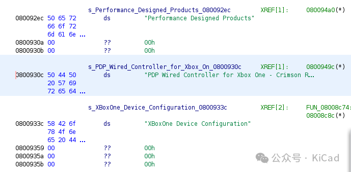
Let’s do a simple patch on the product string, changing it to “Testing Firmware Patch”. The following command can be used in the OpenOCD telnet console to overwrite the flash:
wrongbaud@wubuntu:~/blog/stm32-xbox$ telnet localhost 4444Trying 127.0.0.1...Connected to localhost.Escape character is '^]'.Open On-Chip Debugger> flash read 0 bank0-orig.bin> flash read_bank 1 bank1-orig.bin flash size = 512 byteswrote 512 bytes to file bank1-orig.bin from flash bank 1 at offset 0x00000000 in 0.007867s (63.557 KiB/s)> stm32f2x unlock 0Target not haltedstm32f2x failed to unlock device> halttarget halted due to debug-request, current mode: Handler External Interrupt(67)xPSR: 0x61000053 pc: 0x0800839c msp: 0x2000ff48> stm32f2x unlock 0stm32f2x unlocked.INFO: a reset or power cycle is required for the new settings to take effect.> reset halt target halted due to debug-request, current mode: Thread xPSR: 0x01000000 pc: 0x080002a4 msp: 0x20010000> stm32f2x mass_erase 0stm32x mass erase complete> flash write_bank 0 bank0-patch.binwrote 262144 bytes from file bank0-patch.bin to flash bank 0 at offset 0x00000000 in 3.744948s (68.359 KiB/s)> reset > There are a few steps here that may not be very reasonable, so I want to explain:
-
Always back up all flash images before attempting to reflash.
-
See point 1
-
The STM32 flash controller has a lock bit that prevents unnecessary writes. This is set in the “option bytes” of the STM32.
-
Fortunately, we were able to unlock the flash, which is sometimes not an option!
For the internal flash of STM32, we need to perform an erase operation before writing.
-
I should add here that if your target is expensive or important, you never want to do this unless you are 100% sure you can restore it to its original state.
We write the patched firmware image and restart the CPU, prompting the following output indmesg
[54691.886194] usb 1-6.4: new full-speed USB device number 14 using xhci_hcd[54691.992411] usb 1-6.4: New USB device found, idVendor=0e6f, idProduct=02a2, bcdDevice= 1.0f[54691.992417] usb 1-6.4: New USB device strings: Mfr=1, Product=2, SerialNumber=3[54691.992420] usb 1-6.4: Product: Testing Firmware Patches[54691.992423] usb 1-6.4: Manufacturer: Performance Designed Products[54691.992426] usb 1-6.4: SerialNumber: 0000AE38D7650465[54691.998102] input: Generic X-Box pad as /devices/pci0000:00/0000:00:14.0/usb1/1-6/1-6.4/1-6.4:1.0/input/input28Awesome – now we have fully extracted the firmware and loaded it into Ghidra, and we are able to modify it as needed… now it’s time to write some macros.
Conclusion
When evaluating embedded systems, you typically want to enumerate and explore all possible interfaces and methods of interacting with the target. Whether your ultimate goal is to find bugs, modify the normal operation of the device, or understand how it works, hardware debugging is very useful. By leveraging hardware debugging, we were able to extract firmware from the target machine, set up a real-time debugger, and modify the firmware. Through this exercise, we also learned how single-wire debugging works and how to use hardware debugging tools to identify, enumerate, and debug unknown CPUs. We also used OpenOCD based on the FT2232H interface to extract firmware images and reflash new firmware onto the target machine.
The original article is reprinted from Wrongband’s Blog, following the CC BY 4.0 License. Click “Read the original” to view the full article.
Note: If you want to receive KiCad content updates first, please click the card below, follow, and then set it as a star.
Common collection summary:
- KiCad 8 Exploration Collection
- KiCad Usage Experience Sharing
- KiCad Design Projects (Made with KiCad)
- Common Problems and Solutions
- KiCad Development Notes
- Plugin Applications
- Release Records