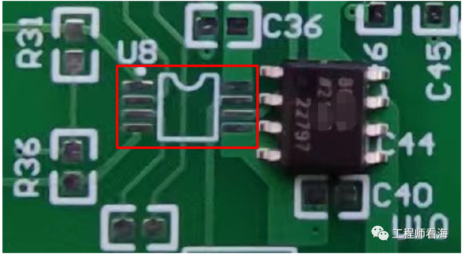
Many people have experienced making mistakes in PCB packaging—either making it too large or too small, or even having components obstructed, which leads to issues when soldering components after the PCB is manufactured, sometimes requiring manual wire connections; in severe cases, it may even result in the entire board being scrapped. For example, the U8 in the image below has a package that is too small, resulting in the chip not being able to be soldered.
So, is there a simple method to check PCB packaging in advance to avoid pitfalls?
Of course there is! First, I will discuss the results, followed by the tutorial.
Results Section
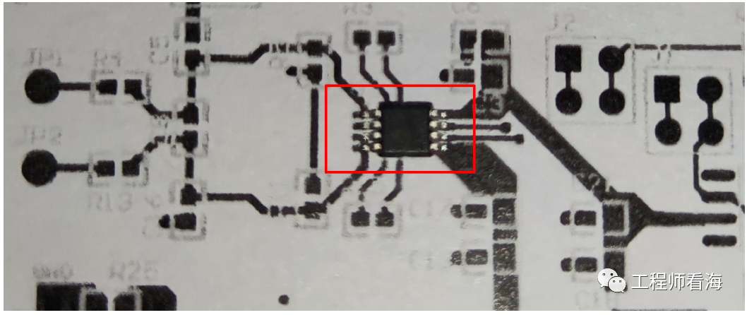
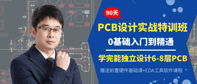
First, print the PCB at a 1:1 scale on paper, then place the components on the paper. This way, you can roughly determine whether the packaging is correct. If it is not correct, make modifications, and once corrected, proceed with manufacturing.
The image below shows the PCB printed on paper, and the chip placed on top for comparison is very suitable.
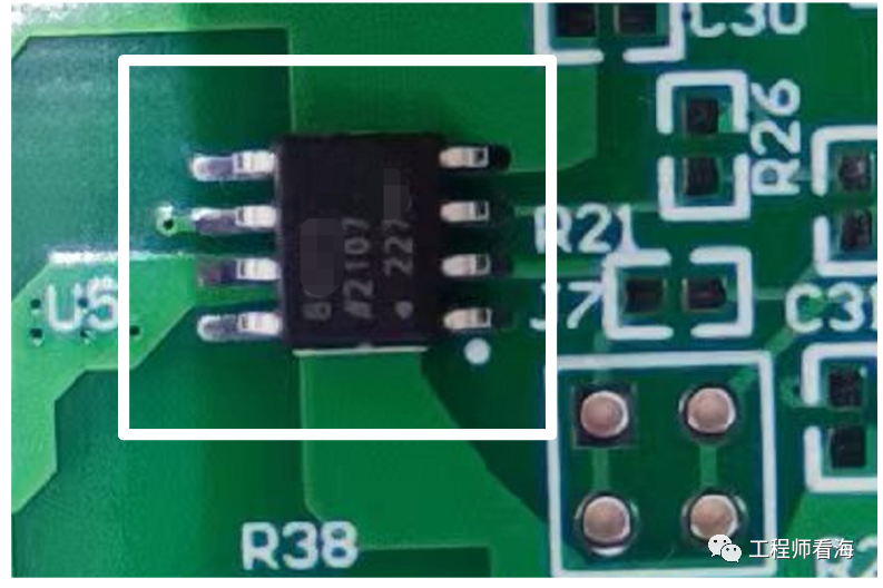
After the board is returned, the dimensions are just right, successfully avoiding pitfalls.
Tutorial Section
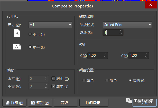
Next, using Altium Designer as an example, I will introduce the printing process.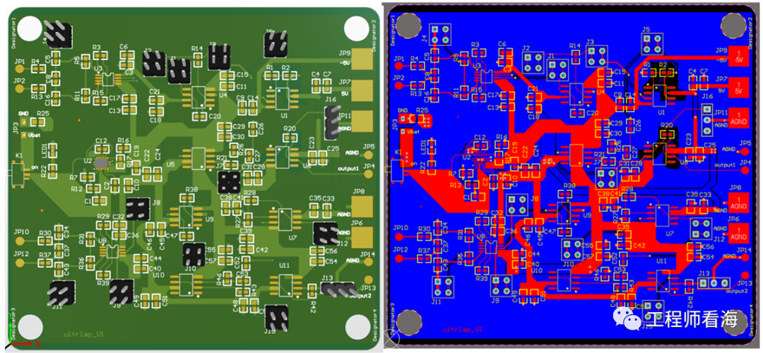 File – Page Setup – Scaling – 1 – Advanced – Remove Background Layer (Print the top layer first, then print the bottom layer, selecting mirror for the bottom layer: Advanced – bottom should be mirrored).
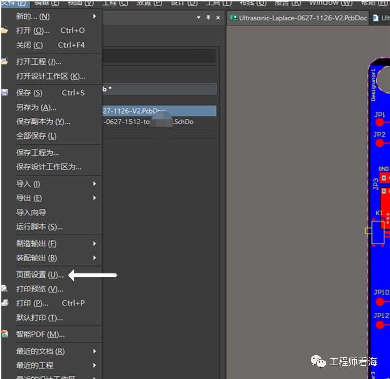
 File – Page Setup – Preview – Print
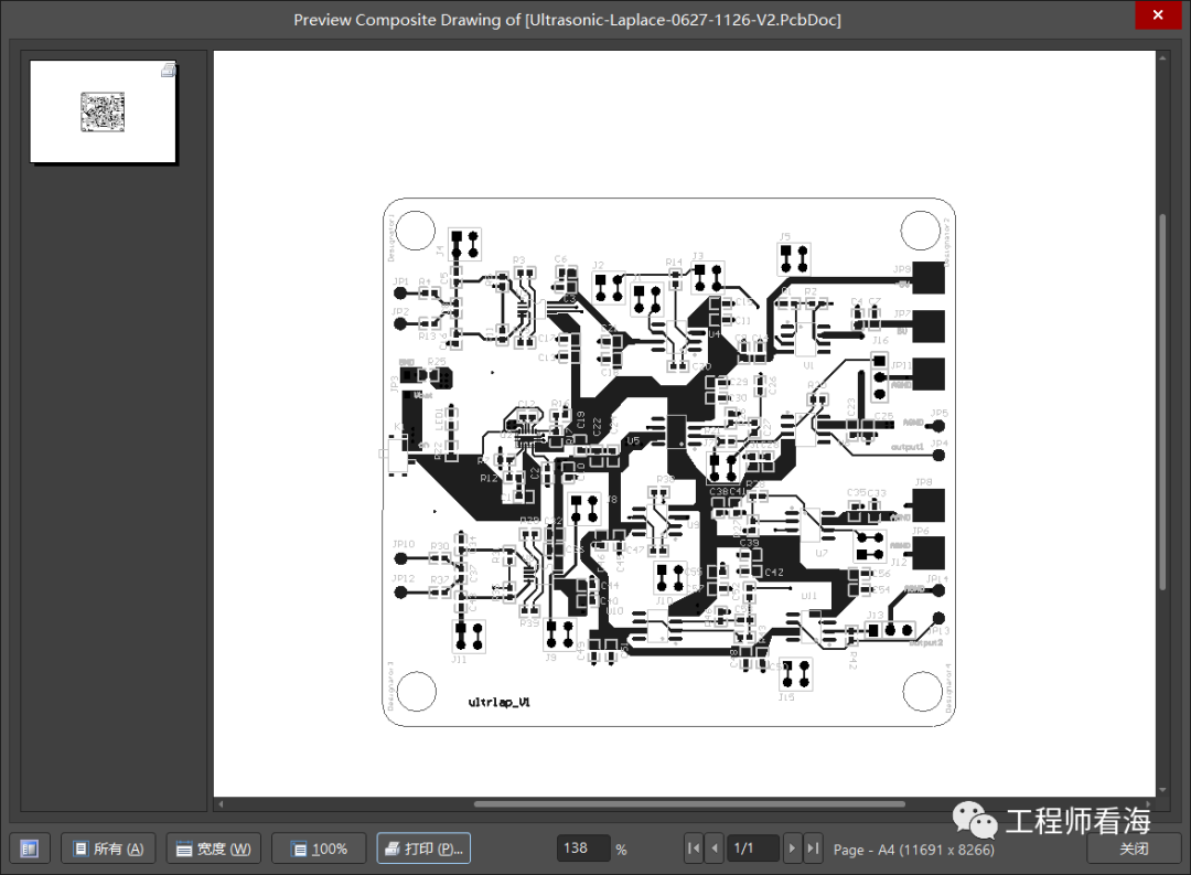 Finally, export as PDF so you can print directly.
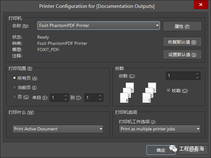 The image below shows the result after manufacturing the board. Isn’t it very simple?
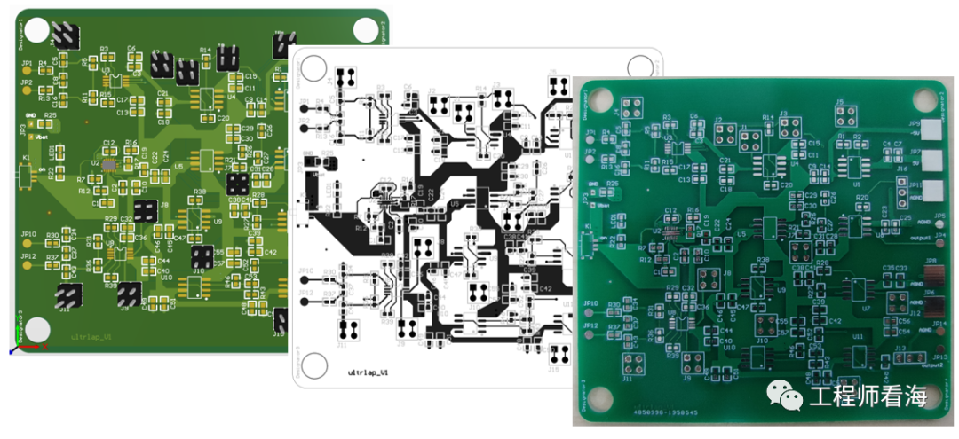 Disclaimer:This article is reproduced from the Engineer’s WeChat account., if there are any issues regarding the content, copyright, or other matters, please contact the staff via WeChat (in0723mango), and we will address it promptly!Submissions/Recruitment/Advertising/Course Collaboration/Resource Exchange, please add WeChat: 13237418207
When you start drawing PCBs, have you thought about these issues?
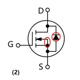
Why do MOSFETs need to be paralleled with diodes?

Scan the QR code to add customer service on WeChat, note “Join Group” to pull you into the official technical WeChat group of Fanyi Education, to discuss technical issues and insights with many electronic technology experts~
Share 💬 Like 👍 Look ❤️ Support with a “triple click”! Click “Read the original” to see more valuable articles.