Click the above“blue text”to follow us!
As a globally renowned memory manufacturer, Micron recently held its 2019 Investor Conference, during which it showcased the development and planning of the next generation of DRAM and NAND Flash technologies.
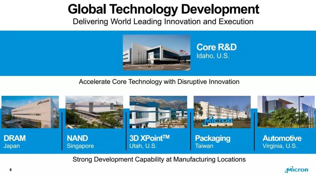
It is reported that Micron’s technology research and Fab manufacturing facilities are spread across the globe, with core technology research primarily concentrated at its Idaho base in the United States. The Fab factories are distributed such that Japan is mainly responsible for DRAM production, Singapore primarily produces NAND Flash, and the 3D Xpoint factory is located in Utah, USA, while Taiwan is responsible for packaging.
Additionally, to meet the demands of the automotive market, Micron has established a factory in Virginia, USA.
Most notably, Micron announced the latest technology roadmap for DRAM and NAND Flash at this Investor Conference.
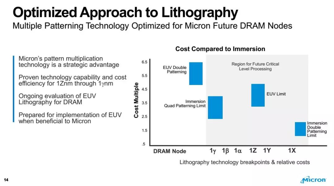
For DRAM, Micron will continue to advance its 1Znm DRAM technology and will also launch a 16Gb LPDDR4 based on this advanced technology. Following the 1Znm DRAM technology, Micron plans to develop 1α, 1β, and 1γ.
In the future, Micron’s DRAM product development plans will adopt EUV technology. Micron stated that it has mature technology and cost-effectiveness from 1Znm to 1ynm, and that multiple exposure lithography technology is its strategic advantage. Currently, the EUV lithography technology for DRAM is under evaluation, with plans to implement EUV technology at the appropriate time.
Regarding NAND Flash, following the 96-layer 3D NAND, Micron plans to develop the next generation of 128-layer 3D NAND, utilizing a 64+64 layer structure.
Furthermore, to lead in chip size, continuous write performance, and write power consumption, Micron will achieve significant progress in transitioning from Floating Gate technology to Replacement Gate technology while continuing to utilize CuA (CMOS under Array) technology during the development of 128-layer 3D NAND.
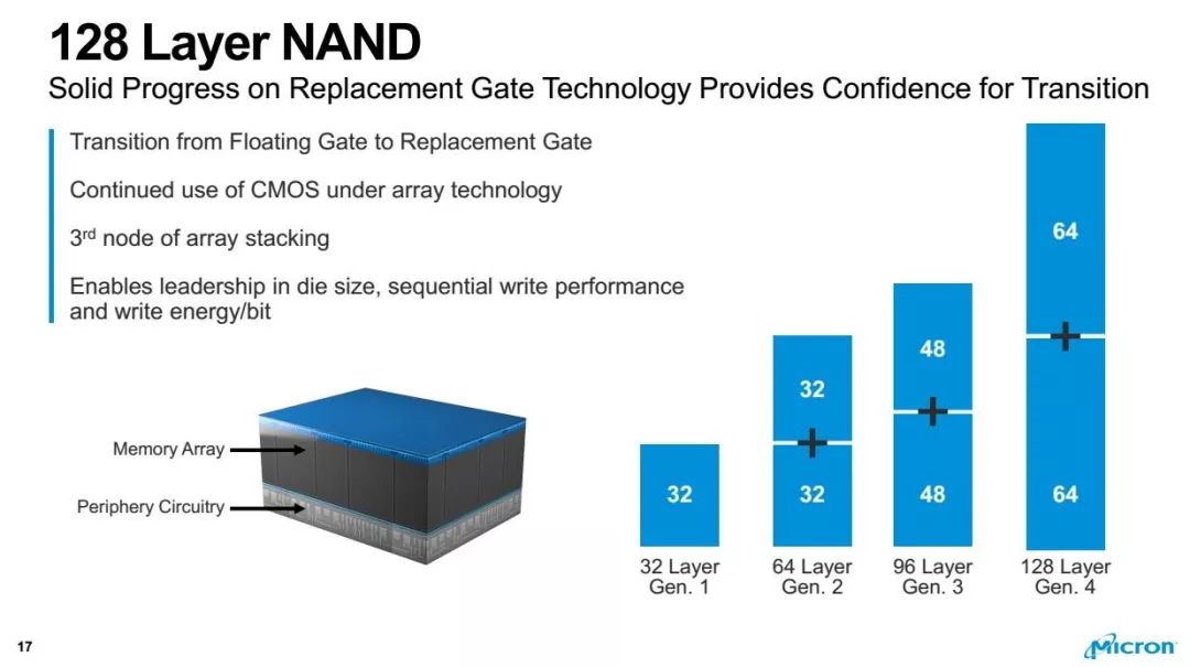
Image statement: Cover image sourced from a legitimate image library, Pai Xin Wang.
Extra:Dear global semiconductor observers, to avoid missing semiconductor industry news due to WeChat updates, please take a moment to set us as a star mark! The specific method is as follows: 1. Click “Global Semiconductor Observation”; 2. Click the top right corner of the public account “…”; 3. Set the public account as a star mark.
PS: If you are using an old version, you can also do this, just click “Pin to Top” in the third step!
Recent Hot Topics
-
Q1 Global Top Ten Packaging and Testing Companies Revenue Ranking: How did the three giants in the mainland perform?
-
35.9 billion: Jita Semiconductor’s specialty process production line project building structure topped out
-
Toshiba Memory and Western Digital invest in K1 factory, producing 96-layer 3D NAND next year
-
$740 million: Marvell acquires Avera Semiconductor, a subsidiary of GlobalFoundries