Introduction
The I2C (Inter-Integrated Circuit) bus is a two-wire serial bus developed by PHILIPS for connecting microcontrollers and their peripheral devices. It is a widely adopted bus standard in the field of microelectronic communication control. It is a special form of synchronous communication, characterized by fewer interface lines, simple control methods, small device packaging, and relatively high communication speeds. The I2C bus supports any IC manufacturing process (CMOS, bipolar). Information is transmitted between devices connected to the bus via the Serial Data (SDA) line and the Serial Clock (SCL) line. Each device has a unique address identification (whether it is a microcontroller – MCU, LCD driver, memory, or keyboard interface), and can act as either a transmitter or receiver (depending on the function of the device). The LCD driver can only act as a receiver, while memory can both receive and send data. In addition to transmitters and receivers, devices can also be viewed as masters or slaves during data transmission (see Table 1). The master is the device that initializes the data transfer on the bus and generates the clock signal that allows transmission. At this time, any addressed device is considered a slave.
Introduction to Hardware Design
I2C Electrical Characteristics:
Pin Definitions: SDA (Data Signal), SCL (Clock Signal)
Transmission Rates: Standard clock 100kb/s, Fast clock 400kb/s, Fastest clock 3.4Mb/s
Transmission Type: Half-duplex
Interface Type: Open-drain (or open-collector) output, requires pull-up resistors
Voltage Levels: Determined by the chip’s voltage, commonly 1.8V, 3.3V, 5V; different voltage levels require level shifting.
Transmission Line Impedance: No requirements;
Allowed Parallel Capacitance: Total equivalent capacitance of the line should not exceed 400pF;
Supported Device Count: Limited by the total line capacitance; adding bus drivers can increase the bus capacitance by ten times, allowing transmission distances of up to 15m.
Application Scenarios: Board-level chips or short-distance communication.
Design Considerations: Level shifting, need for pull-up resistors, increasing bus support through bus drivers.
Typical Level Shifting Circuit:
TR1 and TR2 are both NMOS, Vgate=VDD1, Vth<VDD1, VDD1<VDD2;
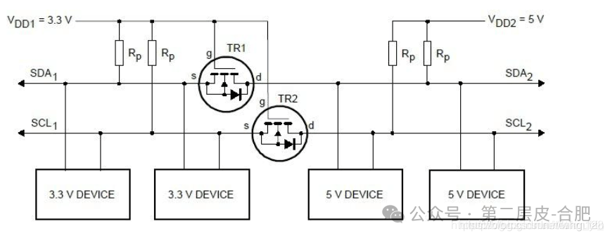
Principle of the Specific Conversion Circuit:
From 3.3V to 5V.
When high, the MOSFET is off, and through the pull-up, it outputs a high level;
When low, Vgs=3.3V>Vgs(th)=1.6V, the MOSFET turns on, is pulled low, and outputs a low level;
In high-impedance state, the MOSFET is off, and through the pull-up, it outputs a high level. From 5V to 3.3V
When high, the MOSFET is off, and through the pull-up, it outputs a high level;
When low, the body diode in the MOSFET conducts, pulling the source low, thus Vgs=3.3V>Vgs(th)=1.6V, the MOSFET turns on, is pulled low, and outputs a low level;
In high-impedance state, the MOSFET is off, and through the pull-up, it outputs a high level.
Relationship Between Pull-up Resistor and Speed
Open-drain structure, so it is required to have pull-ups;
The pull-up resistor for I2C is determined by a calculation formula:
Rmin={Vdd(min)-0.4V}/3mA
Rmax=(T/0.874) *c, T=1us 100KHz, T=0.3us 400KHz
C is Bus capacitance
Rp maximum value is determined by the maximum bus capacitance (Cbmax), and Rp minimum value is determined by Vio and pull-up drive current (maximum taken as 3mA);
Thus, Rpmin=5V/3mA≈1.7K(@Vio=5V) or 2.8V/3mA≈1K(@Vio=2.8V)
In standard mode, the maximum load capacitance for a 100Kbps bus is <=400pF; in fast mode, the maximum load capacitance for a 400Kbps bus is <=200pF. Based on specific usage, current device manufacturing processes, PCB trace distances, and the standard’s backward compatibility, the design is based on fast mode, i.e., total bus load capacitance <200pF, which means achieving a transmission speed of 400Kbps is not a problem. Therefore, the range for Rpmax can be taken as 1.8K~7K @ Vio=5V corresponding to 50pF~200pF.
Based on the limits of Rpmin and Rpmax, a common choice is 5.1K @ Vio=5V, which easily meets the load capacitance requirements. In a 2.8V system, the console design selects 3.3K, while portable/handset low-power designs select 4.7K, sacrificing speed for battery life.