Skip to content
Half Dimension – w Mu Xiaojiu w
Low Power Design Techniques – Multi VDD
Dynamic power consumption is proportional to the square of the voltage; therefore, reducing the supply voltage is very effective in lowering dynamic power consumption. The principle of multi-supply voltage is shown in the figure below. For certain modules in the design, if their functions are relatively independent and there are no very critical timing paths inside, we can lower their supply voltage to reduce dynamic power consumption while ensuring that the timing requirements are still met. For those modules with critical timing, we still let them operate at high voltage to ensure high performance.
In this way, the design can have two or even multiple power domains, and how to layout gates from different power domains becomes a problem.
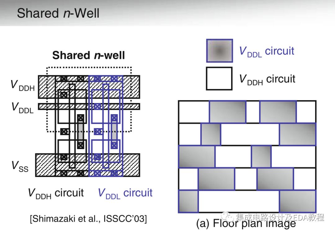
The traditional approach is to place gates with different supply voltages in different Nwell regions (e.g., Low VDD and High VDD).

This approach does not require redesigning standard cells but incurs additional overhead, as space needs to be reserved between the two different voltage Nwell regions.
The most straightforward method is to place cells belonging to different voltage domains together (Dedicated Region), as shown in figure (b). This approach is suitable for the “voltage island” model, where all cells within a module belong to the same voltage domain. It is not very suitable for the custom voltage assignment model, because if a path contains both high-VDD cells and low-VDD cells, the long wiring between different VDD regions will cause additional wire delay, and the extra load capacitance will introduce additional power consumption. Therefore, it is important to ensure that cells connected in the same combination path are within the same voltage domain.
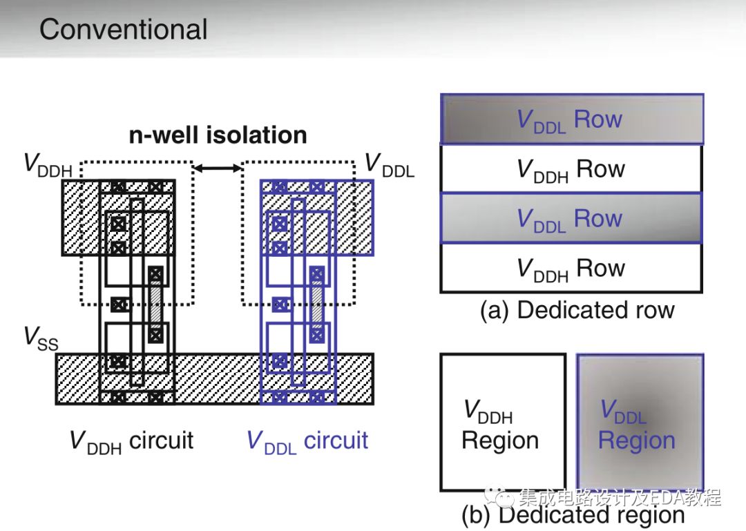
Another solution is to provide a dedicated row for cells in different voltage domains (solution (a)), where each row contains cells of the same voltage domain. This solution is more suitable for “custom voltage assignment”.
Another way to introduce a second power source is to provide each standard cell with two VDD rails, selectively connecting the cells to the correct power source.
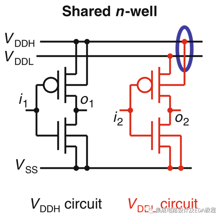
The most universal method is to redesign standard cells in the following manner, where each standard cell has both VDDH and VDDL rails, sharing a common Nwell connected to VDDH. The advantage of this solution is that there is no need to worry about the layout of standard cells; high VDD cells and low VDD cells can be placed next to each other, and the PMOS of low VDD cells is in a reverse body bias state, resulting in lower power consumption. However, the downside is that performance is degraded, and each cell incurs additional area overhead.
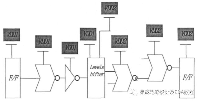
High-speed adder/ALU circuit, Shimazaki et al [Shimazaki, ISSCC’03]
Additionally, if there are signal nets between different power domains, level shifters need to be inserted, and if some power domains may be shut down, isolation cells are also required. The content regarding both will be introduced in future posts.
“Low Power Design Essentials, Jan Rabaey.”
“High-speed adder/ALU circuit, Shimazaki et al [Shimazaki, ISSCC’03]”
# This public account has a red envelope and resource benefitsWeChat Group #
# You can add me on WeChat first, and I will pull you into the group #
# Please add me on WeChat and note the answer to the question below #
If you like this public account, please share it more, thank you for your attention