
Recently, some fans have been asking about knowledge related to Power Gating, such as Switching Cell, Isolation Cell, and Level Shifter. Here I specifically write some articles to discuss these topics.
As 2019 is about to end, how has everyone been this year? Have you achieved your little wishes? 
Low Power Design Techniques–
Power/Ground Gating–
Power Switching Cell
Concept:
Power/Ground Gating is a low power design method in integrated circuits that reduces circuit leakage power by turning off the power or ground of unused modules. This method can reduce static power consumption when the circuit is idle and can also test Iddq.
Theory:
When certain modules in a circuit enter sleep or idle mode, we can use the previously discussed Clock Gating technique to reduce their dynamic power consumption, but we cannot reduce their static power consumption. The Power/Ground Gating technique can completely turn off their power during sleep, thereby eliminating their static power consumption.
In an ideal case, Power gating can completely eliminate the static power consumption of the circuit, but in actual circuits, Power gating can only completely turn off dynamic power consumption, while leakage will only be reduced, not eliminated, because Power gating technology still requires some Always On Cells (such as switching cell, isolate cell, and retention cell, which are always on and cannot be turned off, leading to leakage).
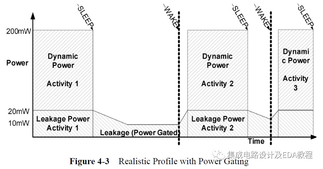
The following figure shows the variation curves of dynamic power and static power in circuits using Power gating in active mode and sleep mode.
Several Cells used in Power gating
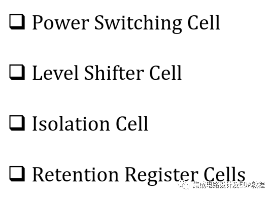
Next, I will introduce several Cells one by one.
Due to the large amount of content and its detailed nature, this article will first introduce the first one–Power Switching Cell.
Power Switching Cell
Selection of Switching Cell corresponding to Power Gating or Ground Gating:
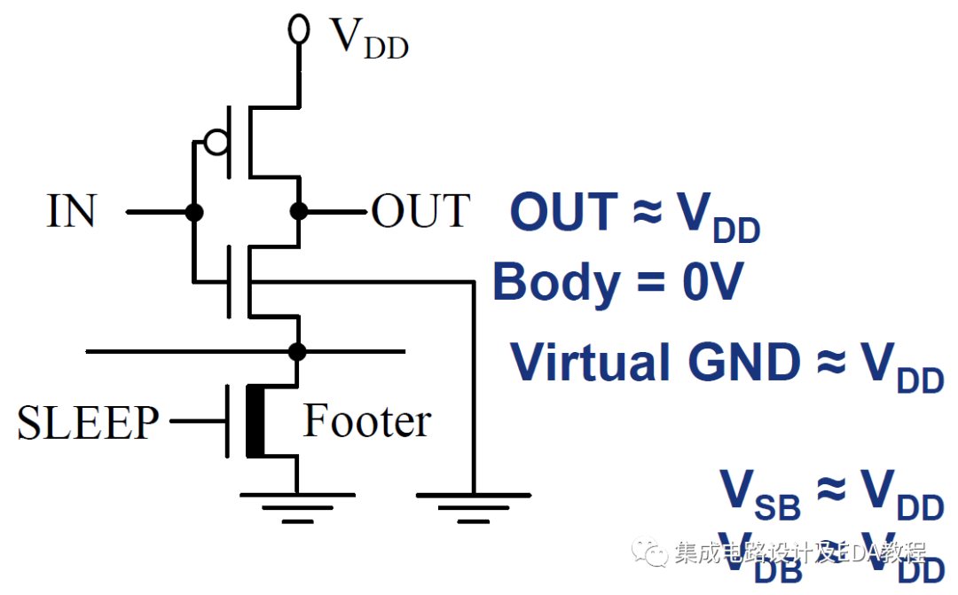
Power Gating -> Header -> PMOS
Ground Gating -> Footer -> NMOS
As Power Switching Cell is an Always On Cell, in order to reduce its power consumption, high-threshold MOS transistors are generally used. In the figure below, the thick black line on the MOS transistor represents high-threshold devices.
The following gives the characteristics, advantages and disadvantages of the two schemes, as well as which gating scheme has lower power consumption in SLEEP mode.
The following figure shows the Power Gating scheme:
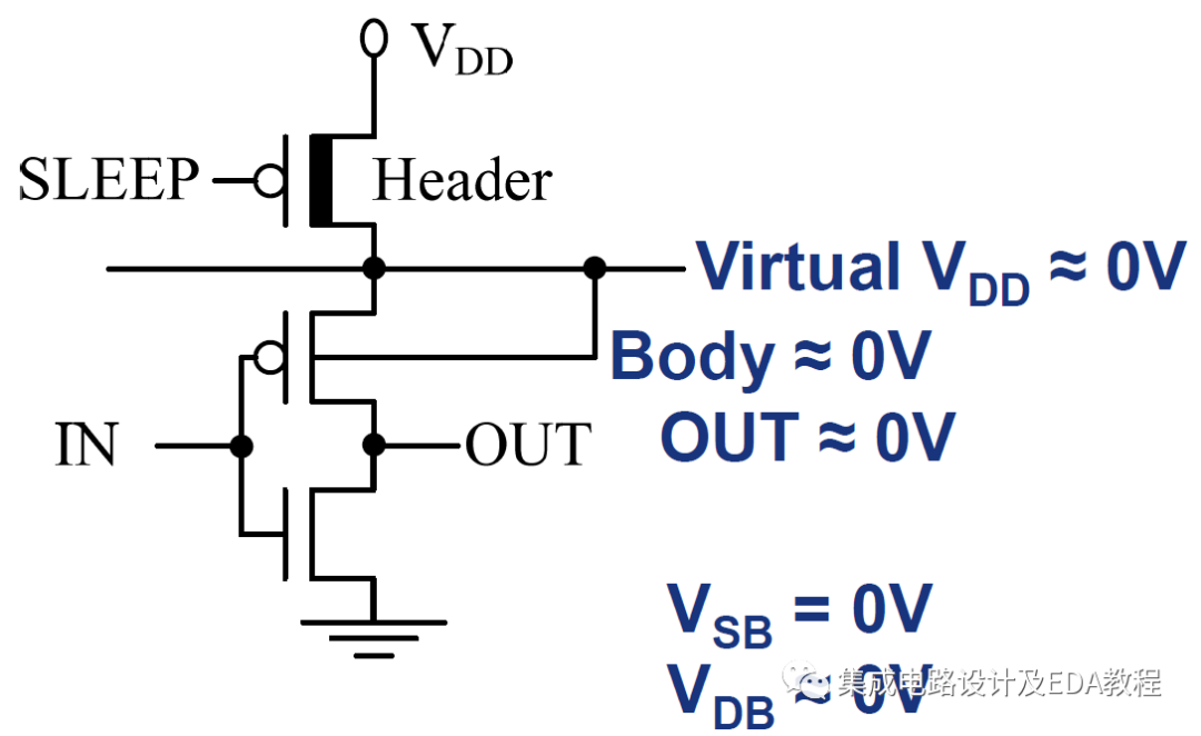
Characteristics:
Header implemented with PMOS, used to control whether the power is connected.
Advantages:
Lower power consumption than Ground Gating implemented with Footer, because the PMOS below the Header (there will be many in actual circuits) is connected to Virtual VDD, which is about 0V in SLEEP mode, avoiding PN junction reverse bias injection current.
Disadvantages:
PMOS drive capability is weak and requires more area compared to Footer. Note: This disadvantage no longer exists in advanced processes; with the introduction of germanium-silicon processes, PMOS may be stronger than NMOS. Since this disadvantage no longer exists, Header is more commonly used in advanced processes, which is Power Gating.
Ground Gating scheme:
Characteristics:
Footer implemented with NMOS, used to control whether GND is connected.
Advantages:
In older processes, NMOS of the same size has stronger drive capability than PMOS, so Ground Gating using Footer is more area-efficient compared to Header. However, in advanced processes, this advantage is gradually lost, as explained earlier.
Disadvantages:
In SLEEP mode, leakage power consumption is relatively high.
Because the NMOS above the Footer (there will be many in actual circuits) is connected to the P substrate, in single-well processes, it can only connect to GND. In SLEEP mode, the potential on both ends of the NMOS source and drain is almost VDD, resulting in significant PN junction reverse bias injection current.
Starting and Stopping of Power Switching Cell
The number, distribution, and starting/stopping of Power Switching Cells are all critical.
This affects IR-drop, timing, leakage current, and the speed of starting and stopping.
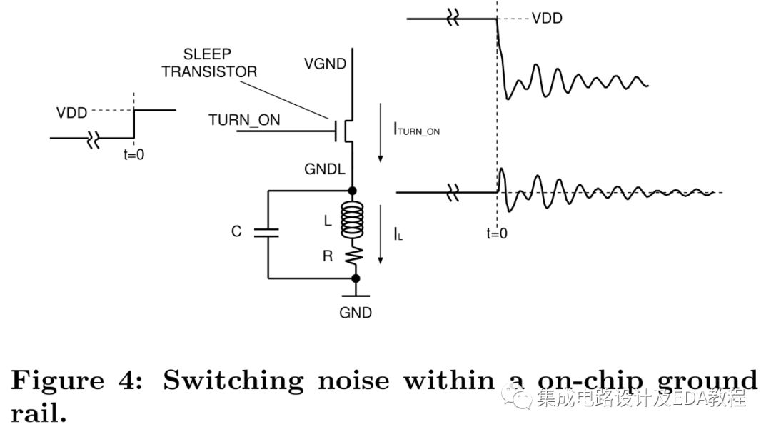
Additionally, all Headers or Footers cannot be turned on or off simultaneously, as this would create significant switching noise on the power or ground, as shown in the figure below:
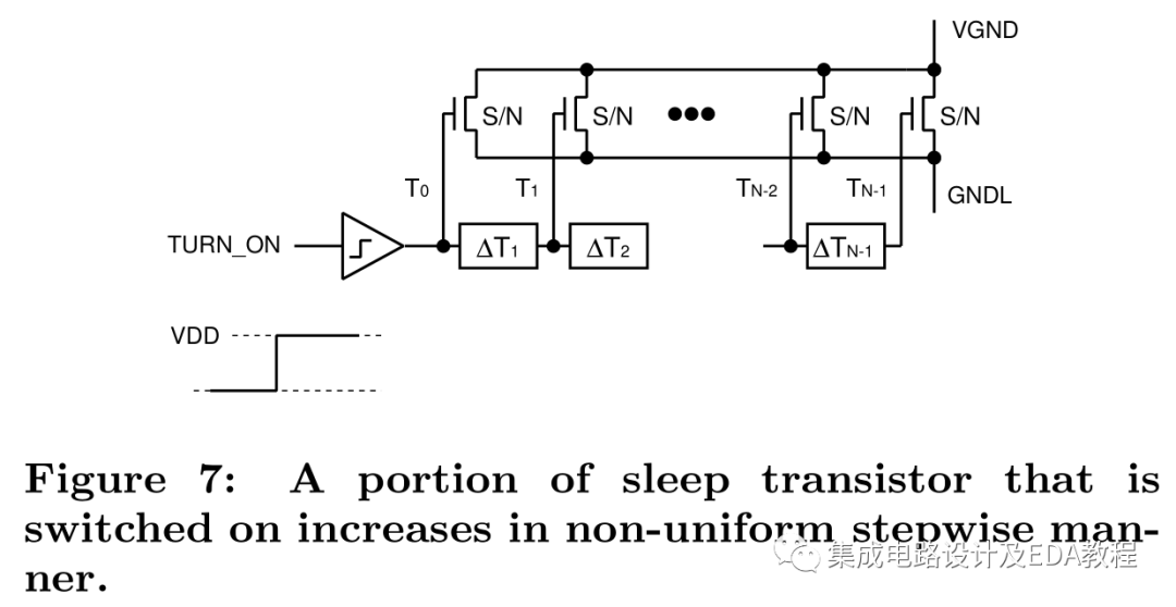
To avoid this phenomenon, current integrated circuit designs widely use the Daisy Chain structure shown in the figure below, inserting Buffers between multiple Footers or Headers, turning on/off one group at intervals, and then another group until all Switching Cells are turned on/off.
Types and Distribution of Power Switching Cell
Earlier, we divided Switching Cells into two types based on Power or Ground Gating: Header and Footer.
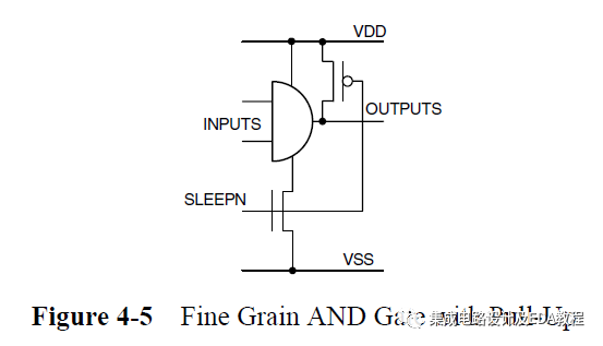
Additionally, we can further divide Switching Cells based on the control form into two types: Coarse Grain Power Switch Cell and Fine Grain Power Switch Cell.
The latter is power control logic designed within some logic units, which is simple but occupies more area, as shown in the figure below:
While the former is discrete Switching Cells that can be controlled in their distribution on the layout, which has a bit more design complexity but less area overhead, this form is widely used now.
According to the content discussed earlier, the distribution of Power Switching Cell in the physical layout has certain requirements.
There is a columnar distribution:
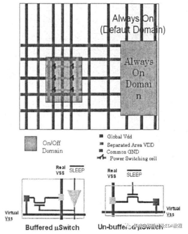
There is also a ring distribution:
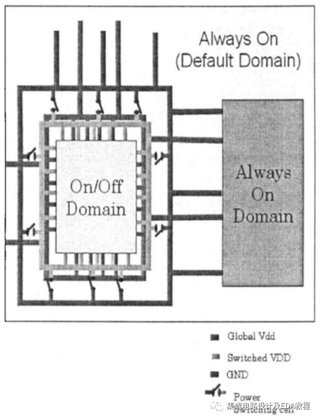
Considering the previously mentioned Daisy Chain structure and factors like IR-drop, columnar arrangement is widely adopted now.
Lib Description of Power Switching Cell
Earlier, it was mentioned that Power Switching Cell has two types: Coarse Grain Power Switch Cell and Fine Grain Power Switch Cell.
Below is a Liberty format description of a Coarse Grain Power Switch Cell:
|
library(<coarse_grain_library_name>) { #Library description starts … lu_table _template ( template_name ) #Voltage state template description, used in dc_current set variable_1 : input_voltage; variable_2 : output_voltage; index_1 ( <float>, … ); index_2 ( <float>, … ); } … cell(<cell_name>) { #Description of a specific Power Switching Cell starts switch_cell_type : coarse_grain; #Switching Cell type is coarse_grain, temporarily only this type is supported … pg_pin ( <VDD/VSS pin name>) { #Declare the format of power and ground pg_pin pg_type : primary_power | primary_ground; #They are primary power and primary ground direction : input ; #Direction is input … } /* Virtual power and ground pins use “switch_function” to describe the logic to shut off the attached design partition */ pg_pin ( <virtual VDD/VSS pin name>) { #Declare internal power and ground, this is the output power/ground port pg_type : internal_power | internal_ground; direction: output; #Direction is output … switch_function : “<function_string>”; #Define the control function for switching, such as SLEEP pg_function : “<function_string>”; #The function of internal power or ground is consistent with the input pg_pin, for header switch it is the primary_power Pin Name, for Footer Switch it is the primary_ground Pin Name } dc_current ( <dc_current_name> ) { #Define the stable current value of the output Pin under different conditions, EDA tools use this data to calculate IR Drop and optimize the Switch. related_switch_pin : <input_pin_name>; #Define the control Pin for switching related_pg_pin : <VDD pin name>; #Define the power Pin that can be controlled for switching, if it is Footer Switch then it is the ground Pin related_internal_pg_pin : <Virtual VDD>; #Define the internal power Pin that will not be turned off, Footer Switch then is the ground Pin values(”<float>, …”); #Define the current value output by this Cell under different states } pin (SLEEP) { #Pin SLEEP description starts, SLEEP is just an example direction : input; switch_pin : true; #Indicates that this input Pin is a switch pin, controlling the power/ground switching … /* The acknowledge output pin uses “function” to represent the propagated switching signal */ pin(<acknowledge_output_pin_name>) { #Definition of acknowledge output Pin starts, after switching, it is consistent with the switch pin state, some Switch Cells may not have this pin … function : “<function_string>”; #Function definition, should be consistent with SLEEP state power_down_function : “function_string”; #Define the power state after shutdown, for Header switch it can be !VDD+VSS, while for Footer Switch it can be !VSS+VDD direction : output; … } /* end pin group */ } /* end cell group */ |
Fine Grain Power Switch Cell’s Liberty format description:
|
cell(<cell_name>) { #Fine Grain Power Switch Cell is part of a specific Cell and does not appear alone is_macro_cell : true; #Define whether it is a macro cell switch_cell_type : coarse_grain | fine_grain; #Most are set to fine_grain pg_pin ( <power/ground pin name>) { #Define power signals, primary_ can be switched off, backup_ cannot be switched off. pg_type : primary_power | primary_ground | backup_power | backup_ground; direction: input | inout | output; … } /* This is a special pg pin that uses “switch_function” to describe the logic to shut off the attached design partition */ pg_pin ( <internal power/ground pin name>) { #Define internal power/ground direction: internal | input | output | inout; pg_type : internal_power | internal_ground; switch_function : “<function_string>”; pg_function : “<function_string>”; … } pin (<input_pin_name>) { direction : input | inout; switch_pin : true | false; #If it is a switch pin, it is true … } … pin(<output_pin_name>) {s direction : output | inout; power_down_function : <function_string>; … } /* end pin group */ } /* end cell group */ |
References:
Dr. Hailong Jiao, Low Power and Variations-Tolerant Digital IC Design in Nanoscale Regime
Design of Power Gating (Overview),https://www.cnblogs.com/-9-8/p/5487239.html
S. Kim, S. V. Kosonocky, and D. R. Knebel, “Understanding and minimizing ground bounce during mode transition of power gating structures,” Proceedings of the IEEE/ACM International Symposium on Low Power Electronics and Design, pp. 22-25, August 2003.
Sun Yiqun, National Technology Co., Ltd., Low Power Physical Implementation Technology for Digital Integrated Circuits and UPF
Cui Yizhi, Fudan University, Application of Low Power Technology in Backend Design