In the wave of AI development, a technology is stepping from the “backstage” to the “forefront”: advanced packaging in semiconductors. This technology enables the integration of chiplets with different functions, processes, sizes, and manufacturers within a single device, creating system-on-chip (SoC) solutions in a flexible, energy-efficient, and cost-effective manner. As a result, more and more AI chip manufacturers are favoring this technology.
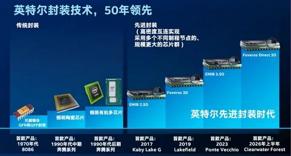
Since the 1970s, Intel has continuously innovated and delved into packaging technology, accumulating over 50 years of rich experience. In the AI era, Intel is collaborating with ecosystem partners and substrate suppliers to jointly establish standards, leading the entire industry in applying advanced packaging technology. Upholding the concept of “System Technology Co-Optimization” (STCO), Intel’s foundry services not only provide customers with traditional packaging, interconnection, and substrate technologies but also encompass system-level architecture and design services, as well as comprehensive support for thermal management and power management.
Comprehensive Technical Portfolio
Intel Foundry’s Advanced System Packaging and Testing (ASAT) technology portfolio includes various technologies such as FCBGA 2D, FCBGA 2D+, EMIB 2.5D, EMIB 3.5D, Foveros 2.5D & 3D, and Foveros Direct 3D.
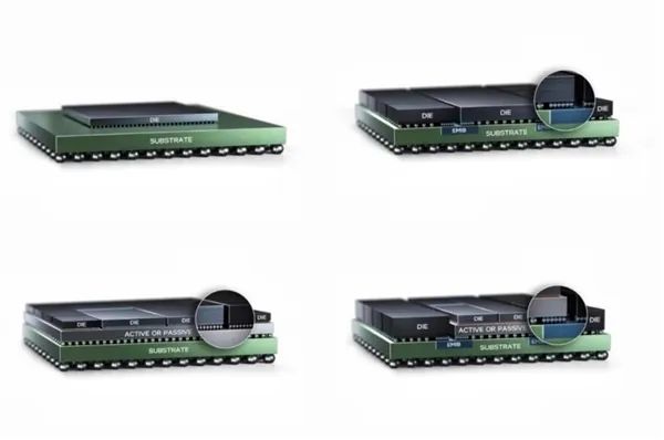 Top left: FCBGA 2D, Top right: EMIB 2.5D, Bottom left: Foveros 2.5D & 3D, Bottom right: EMIB 3.5D
FCBGA 2D is a traditional organic FCBGA (Flip-Chip Ball Grid Array) package suitable for cost-sensitive products with fewer I/O counts. FCBGA 2D+ adds substrate stacking technology, which reduces the area of high-density interconnections, lowering costs, and is particularly suitable for products like networking and switching devices. EMIB (Embedded Multi-die Interconnect Bridge) 2.5D technology connects chips through micro-silicon bridges within the substrate, suitable for high-density chip interconnections, excelling in AI and high-performance computing (HPC) fields. EMIB 3.5D introduces 3D stacking technology, allowing chips to be vertically stacked on active or passive substrates and connected via EMIB technology, increasing stacking flexibility and enabling vertical or horizontal stacking based on IP characteristics while avoiding the use of large intermediary layers. Foveros 2.5D and 3D technologies use solder-based connections instead of substrate connections, suitable for designs that separate high-speed I/O from smaller chip components. Foveros Direct 3D technology achieves higher interconnection bandwidth and lower power consumption through copper-to-copper direct bonding, providing outstanding performance.
It is worth noting that these technologies are not mutually exclusive and can be used simultaneously within a single package, providing great flexibility for complex chip designs. This reflects Intel’s emphasis on the segmented packaging market from a commercial perspective.
EMIB: The Ideal Choice for AI Chip Packaging
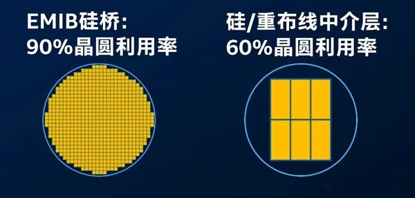
For the advanced packaging needs of AI chips, EMIB 2.5D technology has several advantages compared to other wafer-level 2.5D technologies in the industry, such as silicon interposers and redistribution layers (RDL).
First, cost-effectiveness. The silicon bridge size used in EMIB technology is very small, allowing for more efficient use of wafer area during manufacturing compared to traditional large-sized interposers, reducing space and resource waste, resulting in lower overall costs.
Second, yield improvement. EMIB technology omits the wafer-level assembly step, reducing the risk of yield loss from complex processes such as molds and bumps, thereby improving the overall yield of the production process.
Third, production efficiency. Compared to wafer-level technologies, EMIB technology has fewer manufacturing steps and lower complexity, resulting in shorter production cycles, saving valuable time for customers. In a rapidly changing market environment, this time advantage helps customers obtain product validation data faster and accelerate time-to-market.
Fourth, size optimization. Wafer-level technology requires adding an interposer on top of the substrate, while EMIB embeds the silicon bridge within the substrate, greatly improving the utilization of substrate area. Additionally, the substrate size matches the format of integrated circuit panels, allowing for the integration of more chips within a single package, accommodating more workloads.
Fifth, supply chain and capacity. Intel has a mature supply chain and sufficient capacity, ensuring that EMIB can meet customer demands for advanced packaging solutions.
Looking Ahead
Intel is developing ultra-large packages measuring 120×120 millimeters and plans to introduce glass substrates to the market in the coming years. Compared to the organic substrates currently used, glass substrates offer unique properties such as ultra-low flatness, better thermal stability, and mechanical stability, significantly increasing interconnection density on the substrate and bringing new breakthroughs to AI chip packaging.
Intel continues to innovate in advanced packaging technology for the AI era, leading and driving industry development, injecting new vitality into the global semiconductor industry.
【End of Article】 Please be sure to cite the source if reprinted: Fast Technology