Level ShiftersLevel shifters – converting voltage from low to high
Driving logic signals from a low power rail to a high voltage rail is a critical issue. Under-driven signals can lead to degraded rise and fall times at the receiving end. This, in turn, can result in higher switching short-circuit currents and reduced noise margins. Slow transition times mean that signals linger longer around the threshold, increasing the duration of short-circuit currents. This becomes particularly important for clock tree buffers, as any variation in rise and fall times across voltage domain boundaries increases clock skew.
Specially designed level shifting units address this issue. They provide fast, full-rail signals for high voltage domains. They can be accurately modeled using design tools to achieve precise timing.
There are many design techniques for level shifting, but a simple and straightforward design is shown in Figure 3-2. This design uses a buffer and inverter form of the low voltage signal to drive a cross-coupled transistor structure operating at a higher voltage.
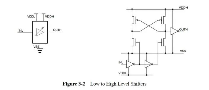
Level shifters require two power rails, typically sharing a common ground. The well structures cannot be connected together and must be independently tied to their respective voltage sources.
These specialized low-to-high level shifters are characterized by matching the operating points of high-side and low-side voltage domains across an extended voltage range. This allows for accurate static timing analysis between different voltage and operating conditions.
Compared to simple buffer delays between low-to-high and high-to-low level shifters, significant delays are introduced. At the interfaces between critical timing blocks—such as between a CPU and cache memory operating at different voltage supplies—designers must consider interface delays and any physical routing constraints crossing voltage boundaries.
Placement of Voltage Converters
Multi-voltage designs present significant challenges in layout. Figure 3-3 shows an example of two voltage domains with a third voltage domain embedded.
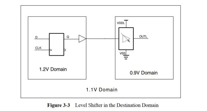
Since high-to-low level shifters use the voltage rail of the low voltage domain, they are typically placed within the low voltage domain. If the distance between the 1.2V domain and the 0.9V domain is small enough, and the library has strong enough buffering, then the driver buffer can be placed in the 1.2V domain without needing additional buffering.
Adding extra buffering in the 1.1V domain clearly presents issues—what power source does the buffer use?
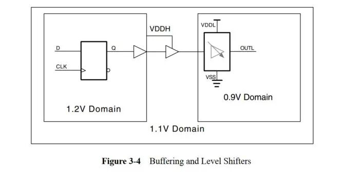
One solution is shown in Figure 3-4. Here, the buffer uses the power rail of the 1.2V domain. However, this means that the 1.2V rail must be routed within the 1.1V domain. This complex power routing is one of the key challenges in automating multi-voltage designs.
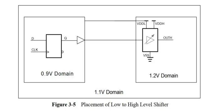
Figure 3-5 illustrates the case where a signal transitions from the 0.9V domain to the 1.2V domain. In this case, regardless of where the level shifter is placed, the power layout routing will be a challenge. Since it requires two voltage sources, at least one voltage rail must be routed from another domain. Because the output driver requires more current than the input driver, we place the level shifter in the 1.2V domain.
Similar to high-to-low voltage converters, if the distance between the 1.2V domain and the 0.9V domain is small enough, and the library has strong enough buffers, then the driver buffer can be placed in the 0.9V domain without needing additional buffering. Otherwise, additional buffering needs to be placed in the 1.1V domain, again leading to the aforementioned voltage routing issues.
Automation and Level Shifters
Level shifters do not affect the functionality of the design: from a logical perspective, they are merely buffers. For this reason, modern implementation tools can automatically insert level shifters where needed without requiring changes to the RTL. Many tools now allow designers to specify a placement strategy for level shifters—placing low-to-high level shifters in lower domains, higher domains, or in between them. Note that output drivers have higher power current requirements; low voltage supplies only need to power weaker devices. Therefore, we recommend placing level shifters in the target domain, as shown in Figures 3-3 and 3-5.
As part of defining level shifter strategies, designers need to specify rules for inserting level shifters. Designers can explicitly specify which blocks require level shifters, or they can specify a minimum voltage difference that necessitates the insertion of level shifters.
High-to-low level shifters should be inserted based on timing considerations. As mentioned earlier, using standard gates instead of level shifters at interfaces between two different voltage domains can lead to erroneous delay calculations. If the voltage difference between the two domains is significant enough, this timing error becomes unacceptable. In such cases, level shifters are necessary. The exact voltage difference depends on the library and design goals.
Low-to-high level shifters should be inserted based on voltage and timing considerations. If the voltage difference between the two domains is significant enough, the input stage of a standard gate in the higher voltage domain will not fully turn off, leading to excessive short-circuit current.
Specifically, if the voltage difference exceeds the threshold voltage of the receiving PMOS transistor, the transistor will not fully turn off. To provide a reasonable noise margin, we should fill this number with 10% of VDDH (the higher supply voltage). Therefore:

Then use a level shifter to turn off the input of the receiving PMOS.
Recommendations and Pitfalls for Using Level Shifters
Recommendations:
Place level shifters in the receiving domain—low domain for high-to-low level shifters, high domain for low-to-high level shifters.
Low-to-high level shifters have significant delays, and these delays need to be understood and carefully considered in the RTL design of critical timing path blocks.
Ensure there is a clear relationship between different voltage domains to clarify whether an up-shifter or down-shifter is needed under operating conditions.
Pitfalls:
Interfaces between domains may be at higher or lower voltages, requiring specialized level shifter components, and making setup and hold time verification at such interfaces very complex.
