Image course, development board –> Taobao store: Wolf FPGA
Consultation WeChat: MyWork666888
QQ group: 543928922
Gigabit Ethernet is a very common solution in FPGA interfaces, and various development boards provide examples in this area. However, the examples provided are mostly based on the RGMII scheme. Today, we will mainly discuss the Gigabit Ethernet solution based on SGMII.Before discussing the specific solution, let’s briefly explain what GMII, RGMII, and SGMII are.GMII is the first standard interface designed for Gigabit Ethernet (1000Mbps), intended to replace the MII interface from the 100Mbps era. It uses an 8-bit wide data bus (TXD[7:0] for transmission, RXD[7:0] for reception),
with one125MHz clock signal for both transmission and reception (GTX_CLK, RX_CLK).
RGMII (Reduced Gigabit Media Independent Interface), translated as the simplified version of GMII, reduces the 8 data lines to 4 while changing the 125MHz clock to a double-edge sampling mode to address the bandwidth reduction caused by the decrease in data width. By using double-edge sampling, it ensures that throughput remains unchanged while using fewer pins to achieve 1000Mbps data transmission.SGMII (Serial Gigabit Media Independent Interface) further reduces the number of pins by using serialization technology, employing1 pair of differential signal lines (LVDS) for transmission,1 pair of differential signal lines for reception. The clock signal is embedded in the data stream (the clock is recovered through 8B/10B encoding), eliminating the need for a separate clock line, thus maximizing pin usage efficiency.From the above explanation, we can see that all three interface schemes can achieve Gigabit data transmission, but the number of pins varies significantly. SGMII uses four lines, two pairs of differential signals, to achieve Gigabit network data transmission with the fewest pins and good anti-interference performance.Today’s discussion on SGMII is based on the 88e1512 hardware, which supports both RGMII and SGMII. The default mode is RGMII, and if SGMII mode is required, some registers need to be configured according to the manual. Below is a reference circuit: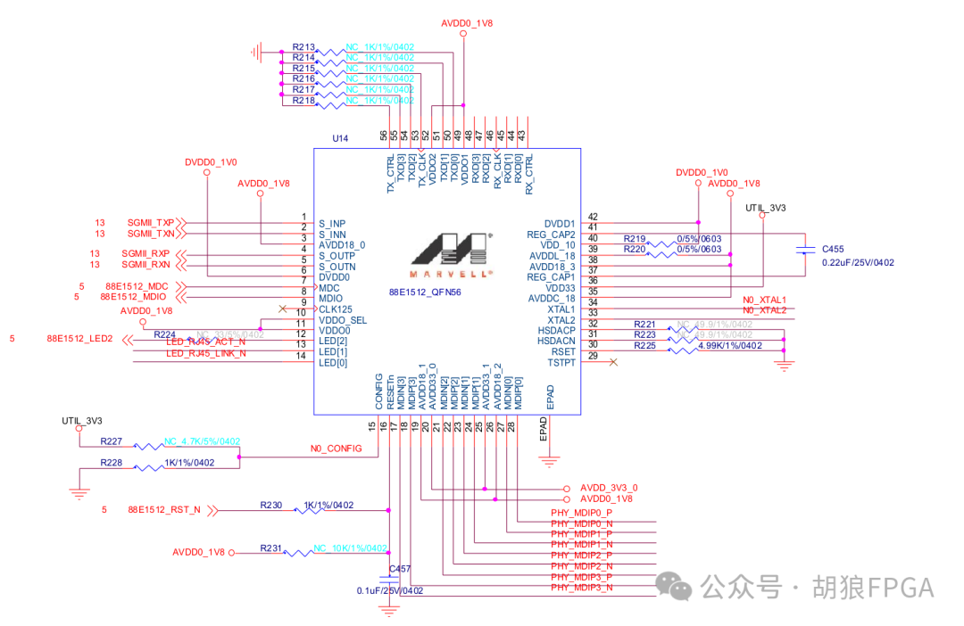 To implement SGMII in FPGA, there are typically two solutions: one is to use devices like MPSoC with ARM cores to output SGMII through PS, or to extend to PL via EMIO. However, if it is a pure logic device, the following method is required:
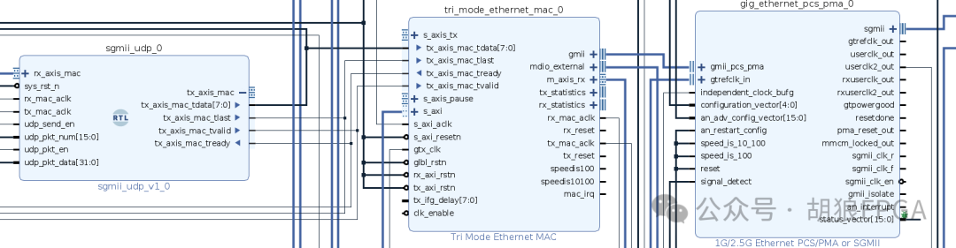 The above figure has three major modules, but to implement SGMII, only the two modules on the right are needed. The TRI mode is the MAC, which outputs GMII data to the rightmost module, which converts GMII to SGMII. The leftmost sgmii_udp module mainly implements the parsing and packaging of ARP and UDP packets required for UDP communication, enabling communication with computers via UDP.That concludes today’s solution. If you are interested in implementation projects, feel free to consult via WeChat at the beginning of the article.
******* Previous Exciting Articles List ********
ISP Algorithm: Medical and Endoscopic Image Enhancement Algorithm
ISP Algorithm: Infrared Image Enhancement
Handwritten Network Protocol: Achieving 100G Network UDP Communication
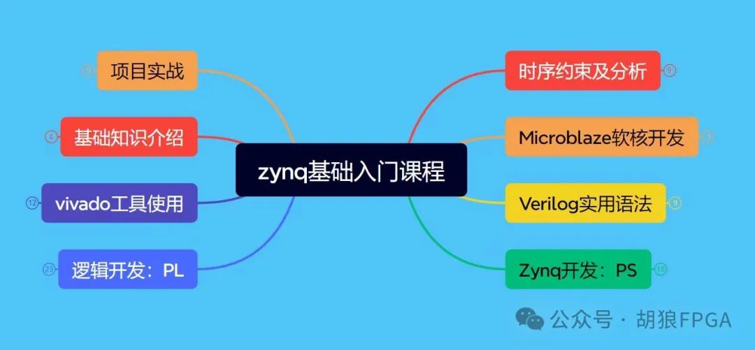
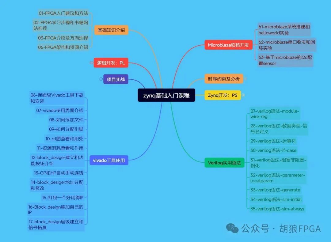
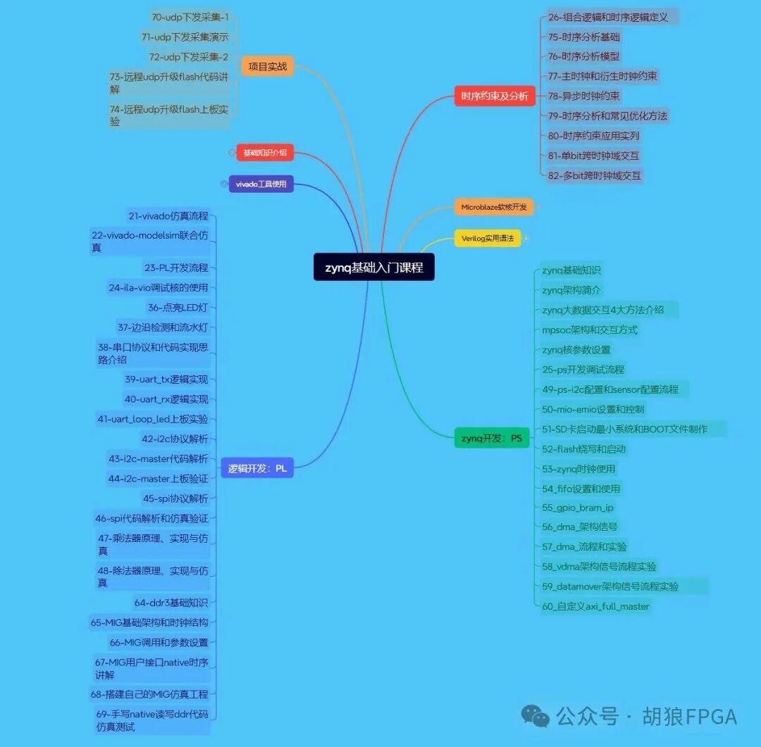
FPGA-Zynq Basic Course Content
Ways to Get Started with Zynq
FPGA Image Algorithm: Image Overlay “Ghost” Logo
FPGA Image Algorithm: Horizontal Stripe Removal
FPGA Image Algorithm: Vertical Stripe Removal Technique
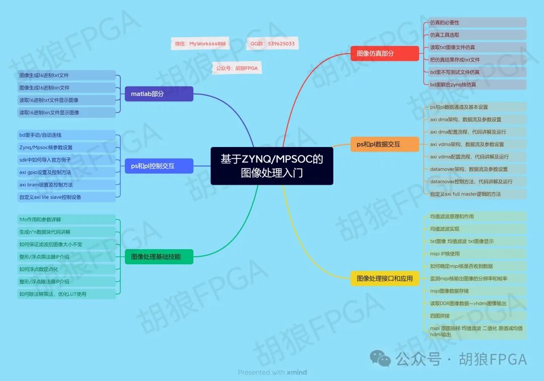
Image Course Collection: Image Skills Course + Image Project
FPGA Course Content Upgrade [Pure Logic and Image Development]
FPGA Image Canny Four Image Stitching Display Project
FPGA MPSOC VCU Compression and Decompression Demo
FPGA Image Arbitrary Scaling. Demo2FPGA Image Algorithm: Arbitrary ScalingFPGA Image Algorithm: Guided FilteringWolf Board 001PLUS Launch, First Release Discount OngoingFPGA Hardware: FMC-HDMI4K-MIPI Interface BoardClick the link above for details