Reading Good Books Together
Laser PFIB Accelerates
Semiconductor Failure Analysis
In the semiconductor industry, with the rapid development of advanced packaging and heterogeneous integration technologies, chip structures are becoming increasingly complex. The widespread application of technologies such as 3D stacking and system-in-package (SiP) presents unprecedented challenges for failure analysis engineers: how to quickly and accurately identify defects or failure points buried deep within millimeter-scale materials?
Investigating the causes of semiconductor failures typically requires the removal of overlying materials to expose the failed circuit components for high-resolution imaging in an electron microscope (EM). Mechanical cutting and polishing techniques can induce mechanical stress, leading to additional defects, and like ion milling techniques, they lack the required point specificity.
The focused ion beam (FIB) can process at specific points, but it is very slow for large-scale tasks. By using laser ablation to remove most of the material surrounding the area of interest, followed by FIB cutting and polishing to obtain cross-sections, the combination of these two technologies ultimately meets the speed and precision requirements for processing large samples. The latest development in this combination is the synergistic processing of laser ablation and plasma-focused ion beam (PFIB) etching to further enhance analysis throughput, efficiency, and flexibility.
Advantages of Laser PFIB Technology
1
Technology Integration
Laser PFIB technology combines the rapid material removal capability of femtosecond lasers with the high-precision processing and polishing capabilities of PFIB, all under real-time imaging monitoring by a scanning electron microscope (SEM). This tri-beam integration technology (Laser, PFIB, SEM) operates on a single co-axial axis, achieving a seamless transition from rapid removal of large amounts of material to final precision polishing and non-destructive imaging.
2
Significantly Increased Material Removal Rate
The material removal speed of femtosecond lasers is approximately 400 times faster than PFIB and about 15,000 times faster than gallium FIB. Combining Laser (initial material cutting) with PFIB (final cutting and polishing) can reduce the total time required for preparing large cross-sections by 95%, and in some cases even more. As shown in Figure 1, the relationship between the spot size and material removal rate of gallium source FIB, PFIB, and Laser is illustrated. The adjacent table provides a numerical comparison of the material removal rates of these three technologies under maximum milling and final polishing beam conditions.
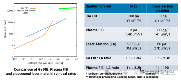
Figure 1: The relationship between the spot size and material removal rate of gallium source FIB, PFIB, and Laser, along with a comparison of material removal rates.
3
Improved Processing and Positioning Accuracy
Dynamic Focusing Homogenized Light Field Technology
By utilizing the nonlinear Kerr effect, the laser focus is compressed to approximately 700 nm and axially extended, achieving ultra-high aspect ratio (1000:1) nano-channel processing.
Co-axial Design
The Laser, PFIB, and SEM beams are located on a single co-axial axis (as shown in Figure 2), ensuring extremely high alignment accuracy and imaging resolution.
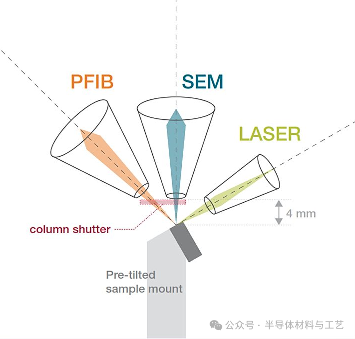
Figure 2: Co-axial design
CAD Navigation and Data Correlation
High-precision area of interest positioning is achieved through the overlay of CAD data based on circuit design or 2D images from various FA tools.
Applications of Laser PFIB Technology
1
Advanced Packaging Analysis
Preparation of large cross-sections for 3D packaged devices, through-silicon vias (TSV), solder ball connections, etc., revealing hidden defects such as micro-cracks, voids, and interfacial delamination. By combining co-axial design with CAD navigation and data correlation technology, precise positioning can be achieved to expose deeply buried defects for high-resolution imaging and analysis.
As shown in Figure 3, the central image displays an ultra-large cross-section, several hundred microns wide and deep, passing through the integrated circuit and connecting to the solder balls and contacts on the inserter. The images on the left and right show details of the cross-section, with the left being a higher magnification image of the IC, and the right showing the gap between the solder ball and the contact pad. The cross-sectioning process took 10 minutes in the laser ablation instrument and 90 minutes in PFIB, saving 70% of the time compared to using PFIB alone.
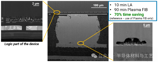
Figure 3: Ultra-large cross-section image of advanced integrated chips
2
Display Device Analysis
Preparation of non-destructive and non-delaminated cross-sections of sensitive devices such as AMOLED mobile displays, which are typically composed of fragile complex materials and structures. Figure 4 shows a case of cross-section testing of OLED using PFIB, where an ultra-large cross-section was cut and polished with PFIB, allowing clear characterization of the morphology and thickness of each vertical layer of the display upon magnification.
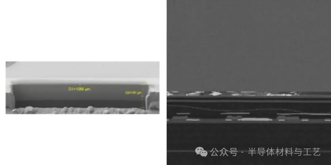
Figure 4: Vertical structure diagram of OLED display:
Top passivation layer – Al electrode – PI layer – ITO layer – PI layer
3
3D Reconstruction
The processing volume of gallium source FIB, PFIB, and Laser increases exponentially over the same time period (as shown in Figure 5), allowing Laser PFIB to achieve millimeter-scale 3D reconstruction through a series of slices and imaging, providing comprehensive structural and compositional information of the device.
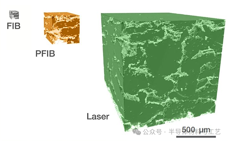
Figure 5: Comparison of processing volumes of gallium source FIB, PFIB, and Laser over the same time period
Laser PFIB technology continues to evolve and innovate, with research into ultrafast laser plasma dynamics making it possible to process ultra-high aspect ratio (1000:1) vertical nano-channel arrays in transparent materials, providing a new processing paradigm for integrated photonics and nano-fluidic devices. The development of these technologies will further enhance the application potential of Laser PFIB in semiconductor analysis, providing analytical solutions for future more complex and precise semiconductor devices.
Main Reference Articles:
1. Thermo Fisher Scientific
2. Jin Jian Optoelectronic Semiconductor Laboratory: How to Efficiently Complete Semiconductor Failure Case Analysis by Combining Plasma FIB Etching and Laser Ablation
3. Biotime: Ultrafast Laser Plasma Dynamics Achieving Precision Manufacturing of Ultra-High Aspect Ratio Vertical Nano-Channel Arrays in Transparent Materials
4. Zhihu Material Testing: Using PFIB (Plasma FIB) for Large Area Micro-Nano Processing