Introduction
Soldering is a crucial process in the manufacturing of electronic devices. The quality of soldering directly affects the performance of electronic circuits and devices. Excellent soldering quality provides good stability and reliability for circuits, while poor soldering methods can lead to component damage, significant testing difficulties, and potential hazards that prevent devices from functioning properly. Therefore, understanding and mastering the necessary soldering skills is very important.
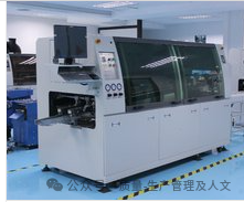
Part Two – Wave Soldering
Wave soldering is a key process used in electronic manufacturing for soldering through-hole components (THT) and some surface-mounted devices (SMD), especially suitable for mixed technology boards (containing both THT and SMD).
Core Principle: A continuous flowing “wave” of molten solder is formed, and when the printed circuit board (PCB) passes through the wave at a specific angle and speed, the solder wets the exposed metal surfaces (pads and component leads), forming reliable solder joints upon cooling.
Typical Process Flow:
1. PCB Loading: – Load the completed SMT reflow soldered PCB (with surface-mounted components) into a fixture to protect the existing SMDs and secure the PCB.
2. Flux Application: Method: Spray (mainstream), foam, or jetting.
Function: Remove the oxide layer and enhance solder wetting.
Key Control: Uniformity of application, thickness (too little leads to cold solder joints, too much leaves corrosive residues).
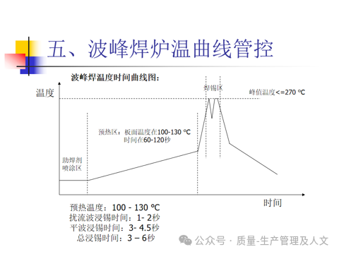
3. Preheating: Purpose: Evaporate solvents in the flux to prevent solder splashing at high temperatures. Reduce thermal shock to the PCB during soldering. Activate the chemical activity of the flux.
Temperature: Typically 80–120°C (measured on the board), time 1–3 minutes.
4. Wave Soldering:
Single Wave: Traditional mode, suitable for pure THT boards.
Dual Wave (mainstream):
Turbulent Wave (Chip Wave): High-pressure turbulence breaks the air barrier under SMD components, solving the “shadow effect.”
Laminar Wave: Smooth flow forms full solder joints, reducing bridging.
Key Parameters: – Solder Temperature: 250–265°C (lead-free solder)
– Dipping Time: 2–6 seconds
– Transfer Angle: 4–7°
– Wave Height: 1/2–2/3 of the PCB thickness
5. Cooling: Air cooling or natural cooling to solidify solder joints and prevent cold soldering.
6. Unloading/Cleaning:
Key Process Control Points:
1. Solder Composition Management: – Regularly test the solder pot composition (e.g., Cu<0.3% to prevent brittleness), add pure tin to compensate for oxidation losses.
2. Oxidized Solder Dross Control: – Use a spiral rod for automatic dross skimming, nitrogen protection, and add anti-oxidation powder.
3. Temperature Curve Optimization:
Insufficient preheating → Inadequate activation of flux → Cold solder joints; excessive preheating → Early failure of flux → Poor wetting.
4. Wave Stability: Fluctuations in wave height >0.5mm will lead to poor solder joint consistency, requiring regular calibration of pump speed.
Besides the fixture, clean flux residues when necessary (depending on the type of flux).
Key Control Requirements:
1. Flux Control: Flux is the most important chemical material in the wave soldering process. It becomes active at temperatures above 100°C (some types at 90°C) and plays a role in removing oxides from the surfaces of the soldered objects and promoting soldering. It is highly volatile, so strict control is necessary to maximize its effectiveness. Key points for flux control include:
1. Specific Gravity: Due to the volatility of flux, its specific gravity must be strictly controlled to prevent changes in quality. Generally, the specific gravity should be measured every 2 hours, and if it exceeds the standard, it should be adjusted with the corresponding diluent to keep it within the normal range.
2. Application Amount: The amount of flux applied is one of the key factors affecting wave soldering quality. If the application amount is too high, the flux cannot completely evaporate during the preheating stage, leading to splashing in the solder pot and soldering defects such as solder balls; if the application amount is too low, the flux will have evaporated cleanly during preheating, leaving no residual flux to promote soldering, which can also lead to short circuits and insufficient solder. Therefore, the application amount of flux must be controlled. A common method is to use thermal paper laid on the board to check the flux application status: if each hole is wetted without obvious outward seepage, the flux application amount is considered appropriate. At this time, the parameters of the spray system, such as air pressure, flux flow rate, and ultrasonic frequency, should be recorded and fixed as process parameters for a specific model.
2. Solder Wave Parameter Control: Through-hole components complete wave soldering as they pass through the solder wave surface, which is the final step in the wave soldering process and has a critical impact on solder joint quality. Only by optimizing the various parameters of the solder wave to the best combination can good soldering quality be achieved. Key points for solder wave control include:
1. Wave Height: Generally, due to differences in PCB thickness, component types, and component distribution density, the adjustment of wave height cannot be standardized. Typically, when the board enters the solder wave, the horizontal line of the wave should reach 1/2 to 2/3 of the board thickness. If the PCB requires a fixture to pass through the oven, the wave height can be adjusted to match the entire board thickness.
2. Solder Liquid Temperature: Temperature is crucial for soldering; whether in reflow or wave soldering, temperature parameters are always one of the most critical parameters. The set range for wave solder liquid temperature is 260 – 270°C; for some very simple boards, it can be set to 255°C, but not lower, or soldering defects will occur. Generally, higher temperatures yield better soldering quality; however, since soldering is completed at high temperatures, all components and materials involved in soldering will experience thermal shock, generating thermal stress internally. If not controlled well, thermal stress can lead to material damage, resulting in good soldering quality but poor performance in subsequent testing. Therefore, the adjustment of solder liquid temperature must adhere to the principle of lowering rather than raising. If tests confirm that good soldering quality can be achieved at lower temperatures, the lower temperature value must be set as the standard parameter, and higher temperature settings should not be used.
3. Pin Gap: The pin gap refers to the distance between the bottom surface of the board and the surface of the solder wave nozzle as the board passes through the solder wave. If this gap is set too small, the board may get stuck in the solder oven; if set too large, the motor speed (or frequency) of the solder oven must be increased to create a higher solder wave surface to meet soldering requirements. This will inevitably increase the flow speed of the solder wave, leading to poorer wave flatness, greater variability in soldering quality, and increased oxidation of the liquid solder, resulting in more solder dross. Therefore, the pin gap must be adjusted properly; generally, according to IPC standards, the length of the pin extending from the board surface is 1-2mm, so the pin gap should be adjusted to 3-5mm, with a maximum recommendation of no more than 8mm. This parameter should be optimized to the best value and fixed, not changed arbitrarily.
4. Wave Flatness: Wave flatness is mainly determined by the level of the equipment. Generally, when setting up the wave soldering machine, the entire machine must be leveled, and then the solder pot section must be leveled separately to ensure that the board is level when passing through the solder wave. However, during use, the level may change due to regular maintenance and height adjustments of the solder pot, so regular leveling checks of the solder pot section are necessary. If uneven solder waves are found, adjustments should be made. This work should be included in the monthly maintenance schedule, with inspections conducted monthly. There are two methods for detection: 1) Use a standard high-temperature glass plate to pass through the solder wave and check if the intersection line of the solder wave and the glass is a straight line. If so, the wave flatness is good; if not, adjustments are needed. 2) Measure the distance from the fixed rail and moving rail L-shaped chain claw surface to the solder pot nozzle surface. If equal, the flatness is good; if not, adjustments are needed.
5. Solder Liquid Composition Control: Impurities in the solder liquid can significantly affect soldering quality, so the composition of the solder liquid in the solder pot must be tested regularly. In principle, the solder liquid composition should be tested every 3 months, but monthly testing is preferable. The testing standards can refer to the technical data provided by suppliers.
3. Rail Angle Control: Considering various factors, the rail angle does not have a very significant impact on wave soldering, so this parameter generally does not need adjustment, maintaining it between 5-7 degrees is sufficient. It is recommended to adjust it to between 6.5-6.8 degrees for better results.
4. Chain Speed Control: Chain speed also has a significant impact on wave soldering and affects production capacity. Therefore, adjustments to chain speed should be made cautiously, optimizing it as much as possible and then fixing it, avoiding frequent changes. Chain speed mainly affects the solder immersion time and the final drag soldering state. A faster chain speed results in shorter soldering time but better de-soldering effect; a slower chain speed results in longer soldering time but poorer de-soldering effect. The adjustment range for chain speed is generally between 1.2 – 1.5 meters/minute.
5. Wave Soldering Oven Temperature Curve Control: The temperature curve control points for wave soldering are generally consistent with those for reflow soldering, with the only difference being the requirements for selecting test points and the method of embedding thermocouples. For wave soldering, test points should prioritize components with high thermal capacity. The thermocouples should be welded to ensure that the sensing head is in close contact with the PCB hole ring. Each temperature measurement board should also have a point to detect the board surface temperature of the solder and a temperature sensing line to monitor the solder wave temperature.
Common Defects and Solutions in Wave Soldering
|
Defect Type |
Cause Analysis |
Solution |
|
Bridging (Short Circuit) |
Too close pin spacing, too high wave, too small exit angle |
Optimize fixture design, lower wave height, increase tilt angle (>6°) |
|
Cold Solder Joint |
Insufficient flux activity, low preheating temperature, oxidized leads |
Replace flux, increase preheating temperature, check for material oxidation |
|
Solder Balls |
Excess moisture in flux, insufficient preheating, PCB moisture |
Enhance PCB baking, extend preheating time |
|
Insufficient Solder Penetration |
Large through-hole diameter, high lead thermal capacity, short soldering time |
Increase lead extension length, extend dipping time |
|
Void in Solder Joint |
Poor venting of through-holes, trapped gases from evaporating flux |
Optimize through-hole design, reduce transfer speed |
Emerging Technologies
Selective Wave Soldering: For individual through-hole components, localized soldering through micro nozzles to avoid overall high temperatures (suitable for densely packed mixed technology boards).
Lead-Free Process Adaptation: High temperatures (solder copper nickel alloy melting point ≈227°C) require stronger preheating capabilities and nitrogen protection.
– Intelligent Monitoring Systems: Real-time monitoring of solder composition, wave shape, temperature fluctuations, with AI automatic parameter adjustment.
Summary:
Wave soldering is irreplaceable in soldering through-hole components, with its core being the dynamic control of the interaction between liquid solder and PCB. Process optimization must consider the activity of flux, thermal management, mechanical parameters (angle/speed), and solder maintenance. If you need to delve deeper into solutions for specific defects or equipment selection logic, feel free to ask!
Key Process Control in PCBA Reflow Soldering
Control of Key Processes
Training for Quality Inspectors on Instrument Usage → Use of Network Analyzers
In work, if a certain dimension cannot be measured directly, a dimension chain calculation must be performed, and how to perform dimension chain calculations
Special Process Confirmation and Reconfirmation → Practical Cases
Essential Skills for Mechanical Inspectors – Measurement of Geometric Tolerances
Basic Knowledge Training for Quality Inspectors Five – Common Measuring Tools Usage and Precautions
Basic Knowledge Training for Quality Inspectors Three – Inspection
Basic Knowledge Training for Quality Inspectors Two – Inspection Knowledge
Basic Knowledge Training for Quality Inspectors One – Reading Drawings: