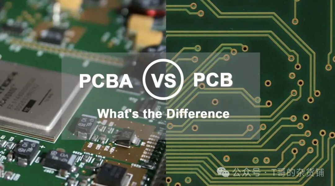
This article will deeply compare PCBA and PCB! We will start with their basic definitions and principles, exploring the key differences in design, manufacturing, and practical applications. You will learn how PCBs are constructed and how they differ from fully assembled PCBAs. We will also explore real-world application cases across various industries, discuss manufacturing and cost considerations, and provide practical guidelines on when to choose one over the other!
Introduction
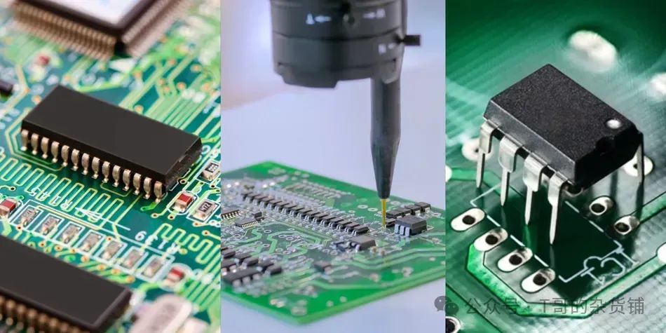
If you have ever peeked inside a smartphone or computer, you have likely seen a green flat board with copper traces and soldered chips. This board is commonly referred to as a PCB, or printed circuit board. However, once all the chips and components are installed, it becomes a PCBA, or printed circuit board assembly. In electronic engineering, the terms PCBA and PCB are sometimes used interchangeably, but they actually refer to different stages in the lifecycle of a circuit board. The differences between PCBA and PCB are not just about assembly—they affect functionality, production processes, and final application scenarios.
This article will deeply compare PCBA and PCB! We will start with their basic definitions and principles, exploring the key differences in design, manufacturing, and practical applications. You will learn how PCBs are constructed and how they differ from fully assembled PCBAs. We will also explore real-world application cases across various industries, discuss manufacturing and cost considerations, and provide practical guidelines on when to choose one over the other!
What is PCB?
A printed circuit board (PCB) is a flat board made of insulating material, etched with conductive copper paths. These copper traces form electrical connections between electronic components.
Essentially, a PCB is a structure that mechanically supports and electrically connects electronic components to form a unified circuit. A PCB typically consists of multiple layers: at least one dielectric substrate layer and one or more copper layers that form the circuit. Electronic components are then installed onto this board, but in its bare state, the PCB has not yet been assembled with any electronic components.
PCB Structure
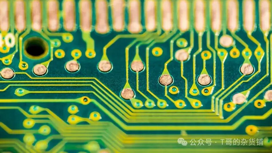
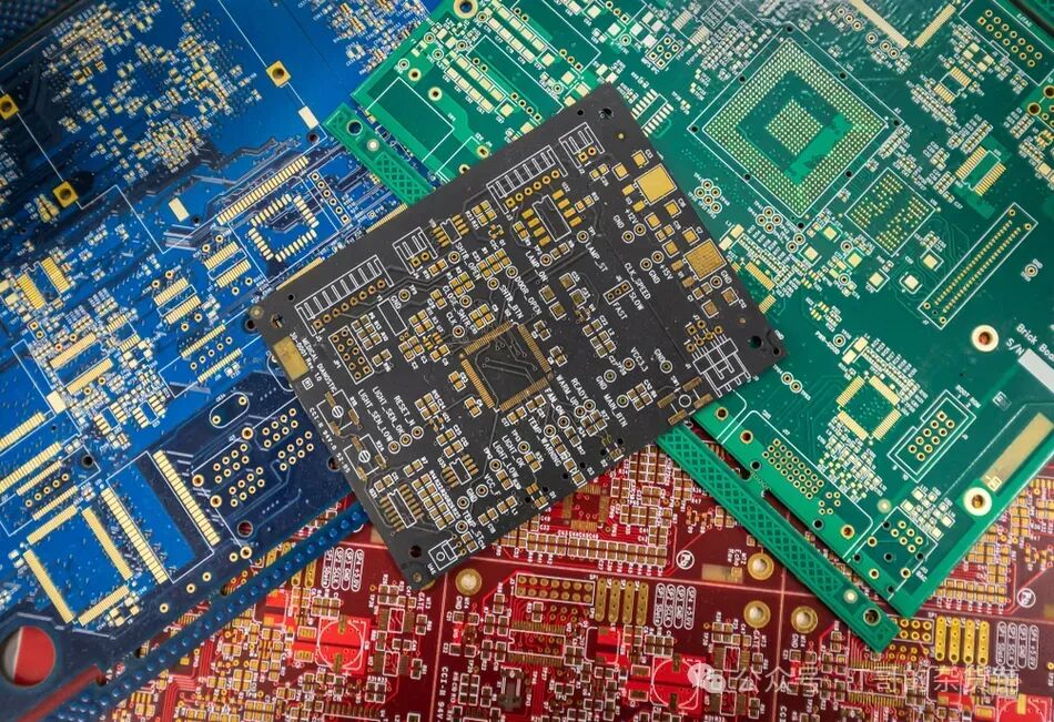
Most PCBs use rigid glass fiber epoxy resin substrate material (commonly with flame-retardant properties, known as FR-4), but flexible PCBs can also be made from flexible plastic films. Copper foil is laminated onto the substrate, and then selectively etched to form copper traces (wires) that connect component pads. PCBs also contain drilled holes—some of which are plated with copper (known as vias)—to achieve inter-layer connections or to mount through-hole components. A protective solder mask (usually green) covers the copper traces to insulate and protect them, leaving openings only where components need to be soldered. White silkscreen labels can be printed on the board to indicate component reference identifiers or symbols.
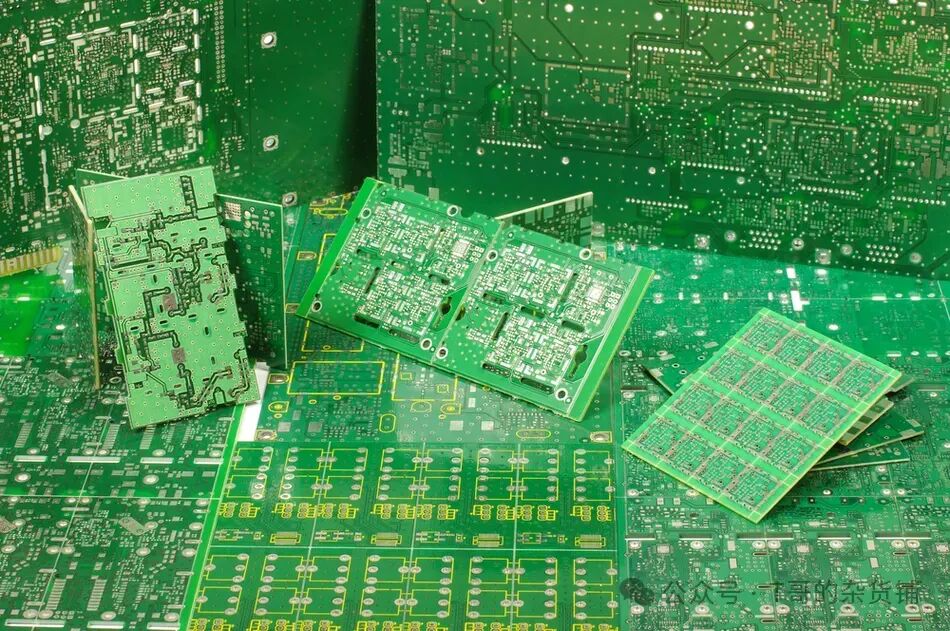
Types of PCBs
PCB designs range from extremely simple to highly complex, and can be categorized into various types based on structure and application.
Let’s take a closer look at them:
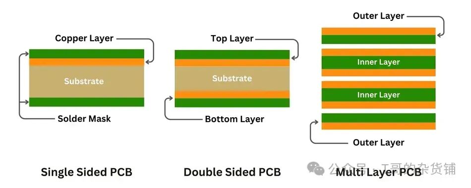
- Single-sided PCB: A PCB with copper traces on only one side of the substrate. Components are typically mounted on the other side. Used for simple electronic products (like basic gadgets, power supplies).
- Double-sided PCB: A circuit board with copper layers on both sides, with a higher wiring density than single-sided boards. Connections between the two sides are made through vias, commonly found in moderately complex circuits (like household appliances, instrumentation).
- Multi-layer PCB: A circuit board with three or more copper layers, separated by insulating materials. Inter-layer connections are achieved through vias (through-hole, blind, buried). Multi-layer PCBs allow for high-density interconnections of complex circuits and are widely used in high-end devices (like computer motherboards, smartphones, commonly 4 layers, 6 layers, or even more than 8 layers). Ultra-high layer count boards (even 50+ layers) are used in server backplanes or aerospace systems to meet extremely complex wiring needs.
- Flexible PCB (Flex) and rigid-flex boards: Flexible PCBs use flexible plastic substrates (like Kapton), allowing the circuit board to bend or fold. Rigid-flex boards combine rigid and flexible parts within the same PCB, commonly used in compact devices (like foldable phones and cameras) to save space and weight.
The choice of each type of PCB is based on application needs. For example, a simple toy may use a single-sided PCB, while a high-end graphics card would use a multi-layer PCB with controlled impedance to support high-speed signal transmission.
Use Cases
Printed circuit boards (PCBs) are fundamental components of almost all electronic devices, widely used in everyday consumer electronics (like smartphones, laptops, TVs, home appliances), industrial machinery, automotive electronics, medical devices, aerospace systems, and more.
Essentially, any electronic device containing multiple components will use a PCB to secure and connect these parts. However, as a bare board, the PCB itself has no functionality until components are added. This is precisely the significance of the PCB assembly stage—transforming a static PCB into a dynamic circuit system.
What is PCBA?
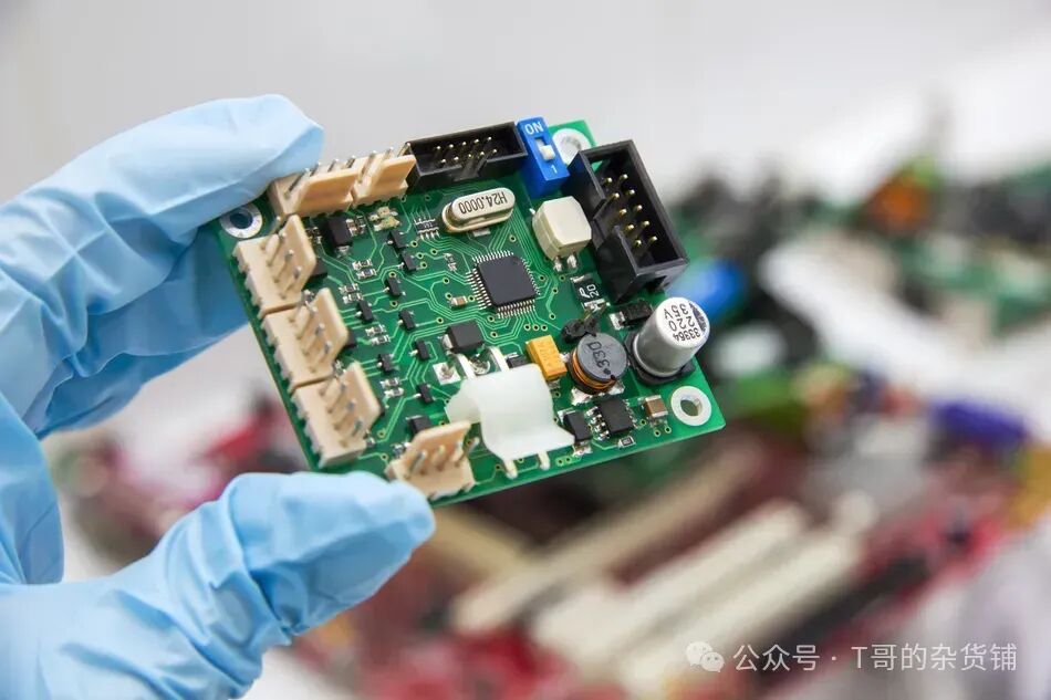
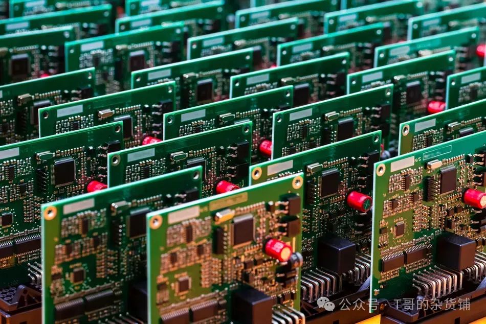
Printed circuit board assembly (PCBA) refers to the finished product after electronic components (such as resistors, capacitors, integrated circuits (ICs), connectors, etc.) are fully assembled onto the PCB. Once all necessary parts are installed and soldered onto the PCB, it becomes a PCBA—a complete circuit board capable of performing its designed functions. In other words, PCBA is the final product of a functional electronic circuit formed after components are installed on the PCB.
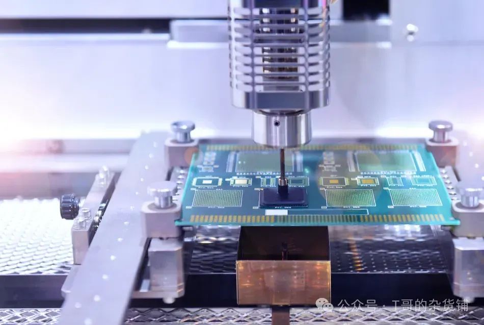
Assembly Process
The process from a bare PCB to a PCBA is called PCB assembly. This process involves multiple steps, primarily achieved through two main techniques.
Let’s understand the basics of these:
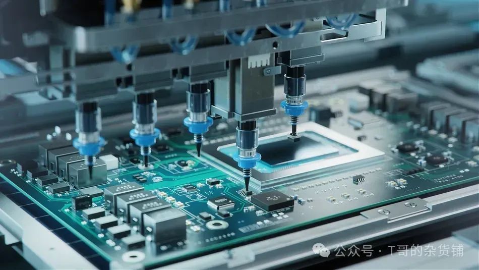
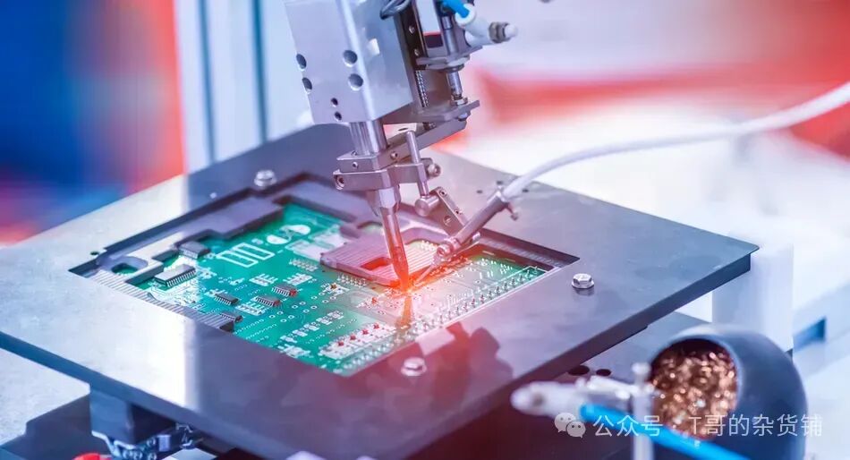
- Surface Mount Technology (SMT): In the SMT assembly process, components (commonly referred to as SMD—surface mount devices) are placed directly on the surface of the PCB pads. First, solder paste (a mixture of solder and flux) is applied to the component pads on the PCB, and then an automatic pick-and-place machine places the SMD components onto these pads. The circuit board passes through a reflow oven, where the solder paste melts and solder connects the component pins to the pads. SMT is very common in modern electronic products because it allows for high component density and can be assembled on both sides of the PCB if needed.
- Through-Hole Technology (THT): In through-hole assembly, components with leads (like traditional resistors, capacitors, or connectors) are inserted into drilled holes on the PCB. These leads are then soldered to copper pads on the other side, either manually or using a wave soldering machine. THT provides a strong mechanical connection (suitable for connectors or components that need to withstand mechanical stress) and is sometimes adopted in harsh environments due to its reliability. However, compared to SMT, it has a lower density and is generally more labor-intensive.
- Mixed Assembly: Many PCBAs use a mixed approach of surface mount technology (SMT) and through-hole inserted components. For example, most small components (ICs, chips, small resistors) are SMT, while connectors or large capacitors may use through-hole insertion. The assembly process may require multiple operations to accommodate both methods.
Typical Assembly Steps
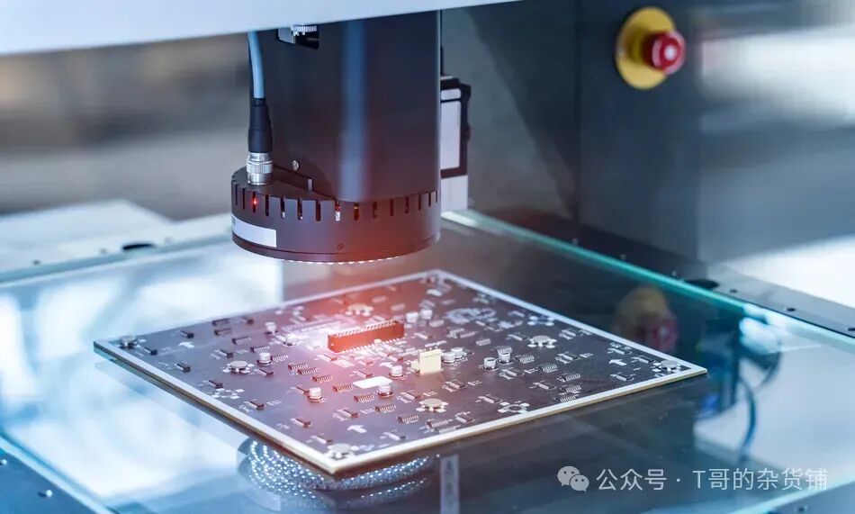
Typical assembly steps include printing solder paste on the PCB pads, placing components, soldering (SMT uses reflow soldering, while through-hole components use wave soldering), followed by inspection and testing. Automated Optical Inspection (AOI) and X-ray inspection (for hidden solder joints like BGA chips) are used to catch soldering defects. Finally, each PCBA may undergo electrical testing, such as in-circuit testing (checking each component/node) or overall functional testing.
Once the assembly is complete, this board is no longer just a PCB—it becomes a PCBA, ready to be integrated into electronic devices or systems. The presence of components means that the PCBA can perform tasks: depending on which components are assembled and how the circuit is designed, the PCBA may be a power module, computer motherboard, or sensor interface.
Importance
PCBA is the true core that drives electronic devices. For example, the PCB inside a smartphone becomes the smartphone motherboard PCBA after all chips (CPU, memory, radio modules) and micro passive components are soldered onto it. This PCBA can start and run the phone. Without assembly, the PCB is just a non-functional object. In informal usage, people may refer to the PCBA in a device as a PCB, but technically, the correct term for an assembled circuit board is PCBA (sometimes referred to as PCA—Printed Circuit Assembly, or CCA—Circuit Card Assembly in industry standards).
Key Differences Between PCB and PCBA
PCB and PCBA are closely related—in fact, they are continuous stages in the electronic manufacturing process—but there are significant differences in definition, design focus, manufacturing, and use.
Comparison: PCB vs. PCBA
Here is a comparison of PCB and PCBA in key aspects:
| Aspect | Printed Circuit Board | PCBA (Printed Circuit Board Assembly) |
|---|---|---|
| Definition | A bare circuit board without installed components, providing electrical connections | A PCB with assembled electronic components, constituting a functional circuit |
| Function | Mechanical support and electrical pathways for components | Performs specific electronic functions |
| Components | None (bare circuit board) | All necessary electronic components (resistors, capacitors, integrated circuits, etc.) |
| Appearance | A flat circuit board with conductive traces, pads, and holes | A circuit board populated with various electronic components |
| Manufacturing | Etching copper layers on the substrate; applying solder mask | Placing and soldering components onto the PCB (surface mount technology, through-hole insertion) |
| Testing | Connectivity and short circuit testing of copper traces | Comprehensive testing (ICT, functional testing) to ensure proper operation |
| Stage | Basic/Foundation | Completed/Functional circuit |
| Application | Used in early design stages, prototyping, and circuit validation | Used in final products like smartphones, computers, and industrial electronics |
PCB is the original, unpopulated circuit board, while PCBA is the finished product that can be put into operation immediately. PCB focuses on the physical design of circuit paths, while PCBA is the actual functional circuit that includes components. A simple memory aid is: PCB + components + soldering = PCBA. In fact, without a PCB, there can be no PCBA—PCB is the first step, and PCBA is built upon it.
Cost and Delivery Cycle
Bare PCBs can be manufactured relatively quickly and at low cost, especially when using standard PCB materials like glass fiber or polyimide. However, it remains incomplete until it is transformed into a printed circuit board assembly (PCBA). The transition from PWB to PCB significantly affects cost and delivery cycles due to the added conductive traces, circuits, and components. Assembling PWB components into functional PCBAs involves surface mount technology (SMT) or point-to-point soldering, increasing costs for components, labor, and testing.
For example, a hobbyist might only spend a few dollars to purchase a small printed circuit board, but integrating copper traces, conductive layers, and components will significantly increase costs. Additionally, industries like high-frequency telecommunications must adhere to strict quality standards set by IPC, further extending production cycles. Wiring choices, dielectric performance, and interconnection methods also affect pricing, making cost optimization a critical aspect of electronic design.
Design Workflow
The electronic product design workflow clearly distinguishes between the PCB and PCBA stages. Engineers first use computer-aided design (CAD) tools (commonly referred to as electronic design automation EDA software) to meticulously design the PCB layout. This critical step involves defining the electrical connections and physical arrangement of components on the circuit board. Once the PCB design is finalized, the next stage moves into manufacturing, which can be achieved through in-house production or by outsourcing to specialized PCB manufacturing services.
The subsequent choice is: engineers can either take on the assembly process themselves, including accurately soldering components onto the PCB, or choose to outsource this task to a professional assembly factory. This assembly step transforms the bare PCB into a fully assembled PCBA.
Practical Applications and Industry Uses
Printed circuit boards (PCBs) and printed circuit board assemblies (PCBAs) are both crucial in the electronics industry, ultimately applied to the same end products but at different manufacturing stages.
Here we explore their practical applications and list examples across industries:
- Prototyping and DIY projects: In early development or educational settings, engineers and students often order bare PCBs. This allows them to manually solder and replace components for testing and debugging. For example, students designing custom Arduino expansion boards may print PCBs and then manually solder components. Bare PCBs are ideal in such scenarios due to their lower cost and the fact that design changes only waste the circuit board rather than assembled components. Reworking or modifying PCBs during the prototyping phase is also more convenient.
- Small batch in-house assembly: Many companies or labs with in-house assembly capabilities will purchase PCBs and assemble them themselves. For example, an electronic startup may produce 100 bare PCBs and have technicians solder components on-site. This approach allows them to control component procurement and adjust assembly processes, making it cost-effective when labor is sufficient and production volume is moderate.
- Turnkey manufacturing: In large-scale production or when time to market is critical, companies often opt for turnkey PCBA services—contracting manufacturers to deliver fully assembled circuit boards. In this case, they receive PCBAs that can be immediately integrated into final products. This is common in consumer electronics and startups without assembly lines; for example, a company designing a fitness tracker may obtain hundreds of assembled PCBAs from a contract manufacturer and only need to place them into plastic enclosures. The advantage of turnkey PCBAs lies in the professional assembly quality and testing (often with warranty/quality assurance).
Industry-Specific Cases
Now, let’s look at industry-specific examples where PCBAs (and their underlying PCBs) are ubiquitous.
Here are some practical application examples:
- Consumer electronics: Smartphones, laptops, TVs, gaming consoles, and home appliances all contain one or more PCBAs (printed circuit board assemblies). For example, the smartphone motherboard is a high-density multi-layer PCBA that houses the processor, memory, radio modules, and sensors. These devices drive PCB technology to achieve fine traces and multi-layer designs while requiring PCBA technology to accurately mount tiny components (like BGA packages with 0.4 mm pitch and 01005 size passive components).
- Automotive electronics: Modern vehicles are filled with electronic devices—engine control units (ECUs), anti-lock braking systems, infotainment systems, sensors, and battery management systems in electric vehicles. All these systems use printed circuit board assemblies (PCBAs). Automotive PCBAs often need to withstand wide temperature ranges and vibrations, so they may use thicker PCBs or special materials, and a mix of surface mount technology (SMT) and through-hole technology to ensure reliability. For example, the PCBA for an airbag control module would use robust PCBs and secure component soldering to ensure it never fails at critical moments.
- Medical devices: From small implants like pacemakers to large imaging equipment (like MRI, ultrasound), medical devices rely on reliable printed circuit board assemblies (PCBAs). Pacemakers embed micro PCBAs that must operate without failure inside the human body for years—this means strict standards for PCB materials (biocompatibility, durability) and assembly quality. The circuit boards of diagnostic equipment are complex, needing to handle sensitive analog signals, requiring careful PCB design and shielding, and comprehensive safety testing for PCBAs.
- Industrial and automation: Factory equipment, robots, and industrial controllers (like PLCs, motor drivers) utilize PCBAs to achieve control and power electronic functions. These circuit boards may use thick copper PCBs to handle high currents, or apply conformal coatings on PCBAs to resist dust and moisture in industrial environments. For example, a motor driver PCBA would use thick copper PCBs and solder power transistors, providing high power handling capabilities.
- Telecommunications: Routers, switches, cellular base stations, and other telecommunications devices all feature high-performance printed circuit board assemblies (PCBAs). These components typically use large multi-layer PCBs with high-speed signal paths and may even include RF components. PCBAs may integrate FPGAs, network processors, and memory chips, all of which require precise assembly. The design and assembly process must ensure signal integrity at high frequencies (GHz range), so material selection and processes are of the highest level (e.g., using controlled impedance PCBs and X-ray inspection for BGA solder joints).
- Aerospace and defense: In satellites, aircraft, and military systems, PCBAs must meet extreme reliability standards. PCBs may be made from special high-temperature or high-frequency laminate materials, and PCBAs may be encapsulated in shielding enclosures. For example, commercial jet avionics systems contain multiple PCBAs for radar, communication, and flight control—each component typically undergoes conformal coating or potting after assembly to ensure reliability. In this field, cost considerations are far less important than absolute reliability and performance requirements.
In these scenarios, the role of bare PCBs is often hidden behind the scenes: PCBs are designed and manufactured by engineers as part of the final PCBA production process. In short, discussions about PCBs focus on the design and manufacturing stages, while PCBAs are delivered and integrated into devices. Whether in consumer electronics or spacecraft, the journey is from PCB design to PCB manufacturing, then to PCBA assembly, and finally deployed in practical applications.
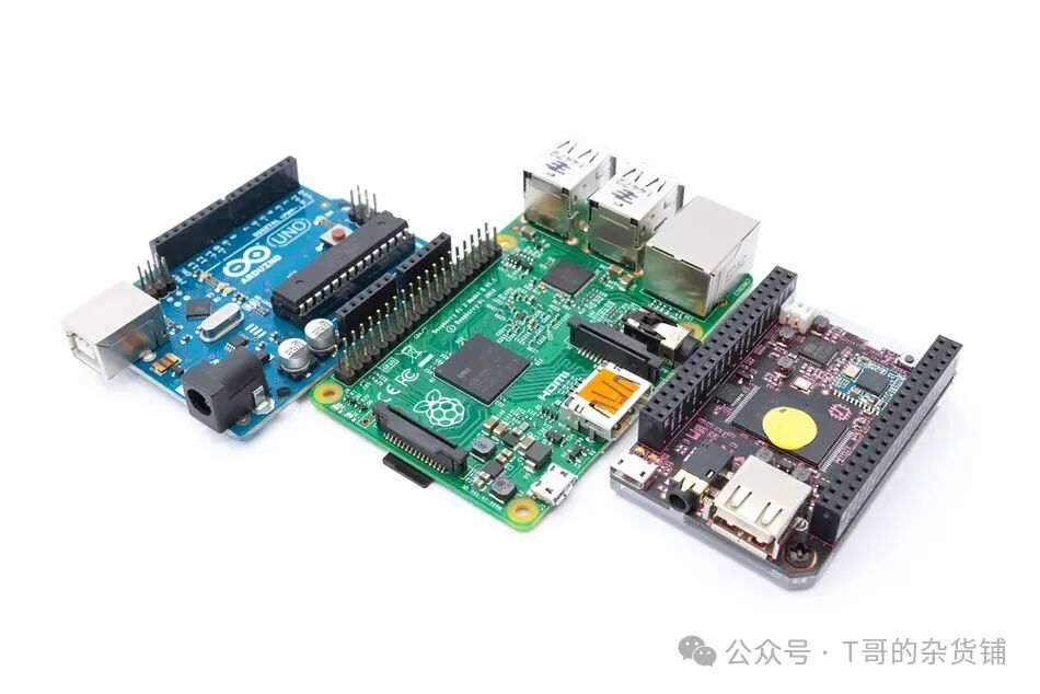
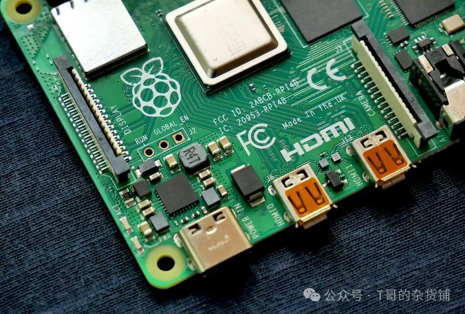
It is worth noting that with the rise of modular electronic devices and development kits, sometimes hobbyists or engineers directly use ready-made PCBAs—such as products like Arduino or Raspberry Pi, which are themselves PCBAs—as components in larger projects. However, these PCBAs are also made from PCBs.
Manufacturing Cost Considerations
When comparing PCBA and PCB from a manufacturing and cost perspective, several factors must be considered: process technology, assembly steps, complexity, and economies of scale. PCB manufacturing and assembly each have their cost structures and challenges, understanding these helps in project planning or product launches.
PCB Manufacturing Costs and Challenges
The cost of producing bare boards depends on several key factors—board size, number of layers, circuit complexity (trace density, minimum line width/spacing), materials, and quantity. Simple double-sided boards made from FR-4 material are relatively inexpensive, especially when ordered in bulk. However, as the number of layers increases or special features are required (like very fine traces, controlled impedance, high-temperature materials, or flexible substrates), the manufacturing process becomes more complex and expensive. For example, a six-layer board will cost more than a double-sided board due to additional lamination steps and material costs. Similarly, adding blind or buried vias or using special RF substrates (for high-frequency circuits) will also increase costs.
Common challenges in the PCB manufacturing process include ensuring layer alignment, drilling a large number of precise vias, and preventing delamination or etching defects. To optimize production and reduce the cost per board, large-scale PCB production employs panelization techniques (i.e., producing multiple circuit boards on each panel). Typically, bare board production is faster and cheaper than complete assembly, as it involves only a single production line operation (involving only circuit board manufacturing). PCB prototype delivery cycles can be as short as a few days, and companies often leverage low-cost PCB manufacturers globally at this stage.
PCBA Manufacturing Costs and Challenges
The cost of PCBA adds multiple additional layers on top of the cost of the PCB itself: component procurement, assembly labor (or machine operation), soldering materials, and testing costs.
Each of these can be critical:
- Component costs: This part can vary significantly. Ordinary resistors or capacitors may cost just a few cents, but specialized integrated circuits or connectors may be worth several dollars or even tens of dollars each. If a design uses a large number of components, the total cost of all parts (commonly referred to as the bill of materials or BOM cost) can dominate. Additionally, component availability is also a factor—if a component is difficult to procure, it may lead to increased costs or production delays.
- Assembly labor and setup costs: If using a contract manufacturer, there will typically be initial setup costs for assembly (programming pick-and-place machines, making solder paste stencils, etc.). This can cost hundreds of dollars or more, which will be spread across the production volume. This means that the unit cost of circuit board assemblies for small batch production may be disproportionately high, as setup costs still need to be paid. In contrast, manually assembling one or two boards can avoid this cost, but is time-consuming and not suitable for fine-pitch or large-scale production. In large-scale production, automated assembly is essential, and as production volume increases (after recovering setup costs), the cost per board decreases.
- Yield and rework: Not every assembled circuit board will pass testing on the first attempt. Complex PCBAs may experience some yield loss (due to soldering defects or component failures requiring rework or scrapping of boards). Manufacturers will factor this cost into their considerations. Design for manufacturability (DFM) practices (good PCB layout, appropriate pad shapes, penalties during assembly, etc.) help maintain high yield rates and reduce costs.
- Testing and quality assurance: Especially for complex or high-reliability products, each PCBA may need to undergo ICT (in-circuit testing) or functional testing. Setting up test fixtures and writing test programs will add costs. However, ensuring that each PCBA works as intended is crucial, especially in industries like automotive or aerospace.
Generally, producing PCBAs is more expensive and time-consuming than PCBs, as it adds additional steps and resources. For example, even if the manufacturing cost of a bare PCB is $5, once you add $15 worth of components and $10 in assembly costs, the cost of the PCBA may reach $30 (these numbers are for illustration only). Producing PCBAs often also extends delivery times: it requires first making the PCB, procuring components (which may have their own lead times), and then assembling and testing. PCBA orders can often take several weeks from start to finish, while bare PCBs may be delivered in a week or less.
Considerations for Large-Scale Production
In large-scale production (hundreds of thousands of units), cost efficiency becomes critical. Typically, PCBs are produced in large panels to reduce the cost per board. Assembly lines are optimized to increase throughput—high-speed pick-and-place machines can place tens of thousands of components per hour. However, challenges still exist: component supply must be reliable (component shortages can halt production lines), and if design issues are discovered later, the cost can be high if a large number of PCBAs have already been produced. Manufacturers may first conduct pilot runs (small batch PCBAs) to validate processes before full-scale production.
Another consideration is that some companies separate PCB manufacturing and assembly to different specialized suppliers (especially when a high-end PCB manufacturer is needed but they have in-house assembly capabilities), while others choose a single supplier for a turnkey solution. There is no one-size-fits-all solution—decisions are based on cost, capabilities, and logistical convenience.
Design Complexity and Its Impact on Manufacturing
The complexity of the design can impact the manufacturing of both PCBs and PCBAs. For PCBs, high-density designs may challenge manufacturing limits (like very fine traces or microvias), which can increase defect rates and manufacturing difficulty. For PCBAs, if there are many fine-pitch components (like ICs, BGA chips, or surface mount components with 0.5 mm pitch or smaller), it means that the assembly process must be precisely calibrated. The more complex the PCBA (number of components, package types, etc.), the more careful the assembly process must be to avoid issues like component tombstoning or BGA misalignment. Design for assembly (DFA) is a key practice: for example, ensuring components are not too close to the board edge (for machine gripping), or that all polarized components are clearly marked to prevent placement errors. Similarly, design for manufacturability (DFM) for PCBs may involve ensuring sufficient spacing, avoiding sharp angles in copper layers that could lead to poor etching, etc.
In terms of cost, design choices have a significant impact: whether to use expensive components or reasonably priced alternatives, or whether to opt for a 4-layer PCB instead of a 2-layer PCB, will directly affect the final cost. Engineers must find a balance between performance requirements and cost constraints. Typically, during the prototyping phase, there may be overspending or less focus on costs; however, for final products that are about to be mass-produced, optimizing designs to reduce costs (while not sacrificing quality) is a key engineering challenge.
In summary, PCB manufacturing is cheaper and simpler, but it is just the skeleton. PCBA is the complete body, requiring more work and cost, but providing full functionality. When planning a project, it is essential to weigh the pros and cons—for example, if in the early design stage, it may be sufficient to order PCBs and manually solder a few key components for testing. This way, when anticipating potential design changes, you can avoid paying for full assembly costs.
However, when you need dozens or more circuit boards, or involve very small components, investing in professional PCB assembly becomes worthwhile. It is crucial to weigh factors such as time, budget, quantity, and internal capabilities. Sometimes a mixed strategy is adopted: assembling critical or complex components in-house while manually soldering some simple components to save costs—everything depends on the specific situation.
Recommended Reading: Design for Manufacturability (DFM): The Ultimate Guide to Optimizing Product Development and Reducing Costs
The Evolution of PCB and PWB
In the early days of electronic technology, printed wiring boards (PWB) were widely used as the basis for circuits, achieving reliable point-to-point connections in circuit design. Over time, the term PWB evolved, and the industry adopted the abbreviation PCB to distinguish between bare boards and printed circuit board assemblies (PCBA) that include installed components. Although the distinction between PWB and PCB still holds significance in some regions like Japan, modern electronics prefer multi-layer conductive layer designs to enhance performance.
The transition to surface mount technology (SMT) and advanced wiring techniques further optimized interconnections, making printed wiring assemblies (PWA) more efficient. Materials like glass fiber, polyimide, and non-conductive substrates enhanced durability, while conductive traces like copper improved signal integrity, especially in high-frequency applications. Historically, polychlorinated biphenyls were used in some PCB manufacturing processes but have been phased out due to environmental concerns. Organizations like IPC have established standards for printed wiring board (PWB) assembly to ensure consistency in electronic design and prototyping across industries.
Recommended Reading:Must-Read for Hardware Engineers: Differences Between PWB and PCB
Conclusion
PCB and PCBA represent the journey from a bare circuit board to a fully functional electronic component. PCB (printed circuit board) is the foundational hardware that provides circuit routing and structure, while PCBA (printed circuit board assembly) brings this board to life by adding components. For digital design engineers and hardware enthusiasts, understanding the differences between the two is not just about terminology—it is about recognizing the different stages of design and production, each with its unique challenges and considerations.
Looking ahead, the fields of PCB design and PCB assembly continue to evolve. PCB technology is advancing (such as high-density interconnect boards HDI, flexible hybrid electronics, and even 3D printed electronics), and assembly technologies are becoming increasingly automated and precise (utilizing robotics and AI inspection). These advancements mean that future engineers will need to be more proficient than ever in layout design and assembly considerations. Design for manufacturability and assembly (DFM/DFA) will play an even greater role in ensuring that PCB designs smoothly transition into reliable PCBAs.
Frequently Asked Questions (FAQ)
1. Are PCB and PCBA the same thing?
No. PCB (printed circuit board) and PCBA (printed circuit board assembly) are related but not the same thing. PCB refers to a bare board that contains only copper traces without any components; PCBA refers to the finished product with all components assembled onto the board. In short, PCBA = PCB + components. You can think of PCB as the foundation, while PCBA is the complete building.
2. What does PCBA include that PCB does not?
A. PCBA includes all electronic components installed on the circuit board, while PCB does not contain any components. PCB provides routing and physical support; PCBA is soldered with resistors, capacitors, chips, connectors, etc. Therefore, PCBA can perform functions (like lighting up an LED, computing data, etc.), while PCB itself cannot achieve any functionality until components are added.
3. Why is PCBA more expensive than PCB?
A. PCBA is more expensive because it includes additional materials and labor. The cost of PCB only covers the manufacturing of the bare board, while the cost of PCBA includes the PCB itself, the cost of all electronic components, and the assembly process (soldering, machine setup, labor, inspection, and testing). Therefore, PCBA costs more and typically has a longer delivery time than PCB. However, PCBA provides a finished and fully functional product, while a PCB alone still requires time and money for assembly.
4. When should I order only a PCB instead of a fully assembled PCBA?
A. It depends on your project needs and capabilities. If you are in the prototyping or development stage and have the ability to solder components yourself, ordering bare boards may be more economical and allow for quicker modifications. This is common for hobbyists or early hardware startups—producing 5-10 PCBs and then manually soldering or partially assembling to test designs. On the other hand, if you need a finished product or have large-scale production needs, ordering PCBA is usually more appropriate.
5. Can I assemble components on a PCB myself?
Yes, if you have the necessary tools and skills, you can assemble components on the PCB yourself. Typically, you will need a soldering iron (or reflow soldering equipment for SMT), solder, tweezers, and possibly a microscope for very small components, along with patience to place components correctly. THT components are more beginner-friendly (just soldering leads), while SMT components may be more challenging, but can be mastered with practice—especially with larger package components.
6. Do all PCB manufacturers offer assembly (PCBA) services?
No, not all PCB manufacturers offer assembly services, but many manufacturers provide them in-house or through partnerships. There are specialized PCB manufacturers focused on producing bare boards; if you send Gerber files, they will return the finished PCBs. Additionally, there are contract manufacturers focused on assembly—submitting PCB designs and bills of materials (BOM) to them, they handle component procurement and assembly (sometimes requiring the customer to provide PCBs, or the manufacturer may produce them).
References
[1] Wevolver. Analysis of FR4 Material and Its Application in PCB Design
[2] Cadence. PCB Assembly and Soldering Technologies
[3] Altium. PCB Design Process: EDA Design Methodology
[4] Viasion. Key Components of PCB: Layers, Traces, and Pads
[5] Acculogic. Introduction to In-Circuit Testing (ICT)
ClickFollow,Make a Friend THE END
The content represents the author’s personal views, and unauthorized reproduction is prohibited.
The opinions and data in this article are for reference only, and any commercial use is at your own risk.
If there are violations or infringements, please send a private message for deletion.
Sharing, liking, and showing love are all encouragement!