
Public Account: Mr. High Speed
Author: Wang Huidong
Longlong, a PCB designer, is working hard and has a beautiful girlfriend named Lily.
However, her mother is adamantly against their relationship. Despite this, her daughter is determined not to give up,
ignoring her mother’s words, until her mother reluctantly agrees to give Longlong a probation period.
If he passes the probation, he can marry Lily; if not, they will part ways.
Lily agrees.
Longlong feels the pressure, but he cannot let his mother-in-law look down on him.
With hope in his heart, he believes he can overcome any challenge.
All good fortune lies in hard work.
Recently, he has a project that needs to be showcased urgently.
Longlong first builds the package and then designs the board, completing the design before production.
Once the materials are ready, they are sent to Company E for soldering and assembly.
Worried about potential issues, Longlong personally delivers the materials to the factory, finally feeling relieved.
However, during the IQC inspection, a small issue arose.
At noon, Longlong received a call from the factory’s IQC.
“Long, we found that the component cannot be seated properly on the PCB during inspection.
Please confirm if there is an issue with this switch component.”
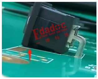
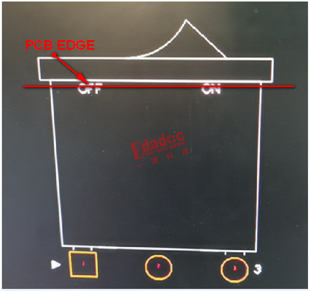
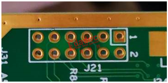
On the PCB, there is a switch component. The IQC followed the silkscreen frame markings on the board, but when they inserted the component, it stood up proudly on the board.
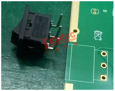
Switch: SWITCH
Package model: KA-0017, specification: sw_4pin, H=4.3mm, H=15mm.
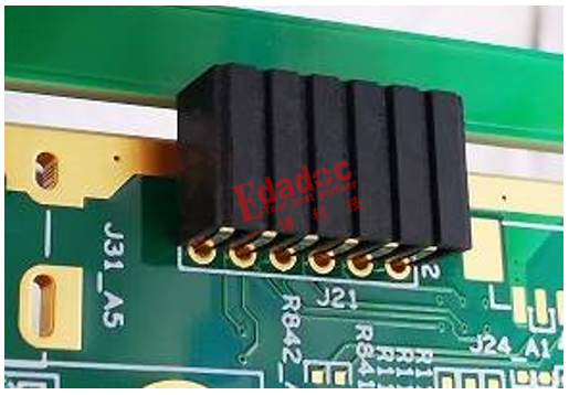
As shown in the image, the switch stands tall and proud on the board.
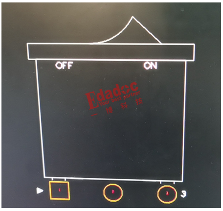
The silkscreen frame markings on the PCB are shown in the image below:
If the switch cannot sink below the board edge after soldering, it will prevent the casing from being installed properly.
The project is urgent, and he is still under his mother-in-law’s probation.
No issues should arise during the probation period.
Thinking of this, cold sweat began to flow down Longlong’s forehead.
In package design, the most feared aspect is the silkscreen frame markings.
In layout design, the most feared aspect is the placement of sinking packages.
In PCB design, drawing lines is not the scariest part; it is the individual effort in building packages, doing layouts, and designing that is truly daunting, as issues in package design can be quite subtle, and one mistake can lead to total failure.
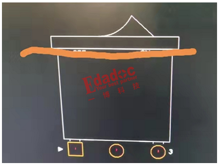
Longlong recalled that when placing components, he did not consider the precise position of the components during assembly, treating the first silkscreen frame as the component’s body.
In fact, this area needs to extend beyond the board.
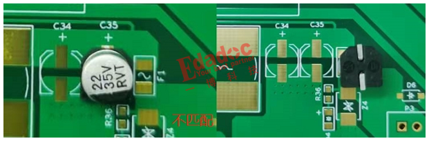
As shown in the image, this is the packaging team at Company E establishing the switch package:
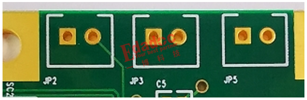
How do we normally place components in PCB layout? In reality, the first silkscreen position should extend beyond the board, while the second silkscreen frame should be close to the board edge, as shown in the image below:
However, there is an important issue to highlight: some PCB design engineers, when building packages, if the position of the second line is the component body, and during layout, if this position is close to the board edge, there is still a significant hidden danger during assembly. This is because we must also consider the dimensional tolerances of the PCB during actual production. Typically, we reference the component layout position based on the second line and extend it more than 0.2mm beyond the PCB edge to prevent interference during assembly due to excessive dimensional tolerances in PCB processing. The white line represents the component body, while the red line represents the PCB edge. Therefore, when designing packages, we need to include a production margin. Based on the material specification sheet, we should indicate the distance from the actual size tolerance to the board edge in the package information. This should be evaluated according to actual production needs, as professional matters should be left to professionals, because focus leads to expertise. For example, the professional packaging team at Company E.
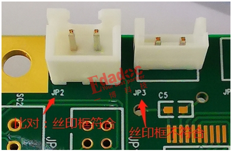
As shown in the image, the red line indicates the board edge position, while the white line indicates the body. Did you add a margin in your package design?
Errors in layout placement lead to tears during rework.
Longlong is anxious.
But no matter how anxious, he cannot make mistakes.
If he makes a mistake, he will disappoint Lily’s eager expectations.
So, Longlong discussed with the factory’s Zhang about emergency countermeasures, to assemble the PCB first and then test it for the exhibition.
Zhang provided a very practical emergency solution: using a reshaping tool to reshape the pins until the switch’s sinking area extends beyond the board, and then assemble the casing. Although it looks a bit ugly, the assembly and testing are fine.
As long as the mindset does not decline, there are always more solutions than difficulties.
The PCB board is always like a girl who can be dressed up; once the casing is installed, no one knows what is hidden inside.
The board later participated in the exhibition and won the bid, and Longlong smiled broadly.
However, through this case, Longlong felt that compared to large PCB design companies, he still feels a significant gap and that there are many professional skills that need improvement.
In fact, there are many times when issues arise due to problems with the silkscreen frame markings during PCB layout and assembly, leading to many confusions.
Next, let’s take a look at these incident sites.
Case 1: As shown in the image, the silkscreen frame for the surface-mounted capacitor is drawn too small, not representing the component body. After layout, the components conflicted, and one was pushed away during soldering. Fortunately, Company E has a material reserve and quickly found a smaller but similar component from the stock warehouse to perfectly solve this issue.
Case 1 involved the component body being designed too small, but even more bizarre is that the component package design is the same size, but the component bodies are different. Please see the image below:
Case 2:
The silkscreen frames on the board are the same size, but during IQC inspection, it was found that the two components were not the same. The IQC suspected that the customer’s components were provided incorrectly.
In fact, the component sizes were different, but the silkscreen frames were the same during package design, which was a false alarm.
Case 3:
There is an even more exaggerated case. Looking at the image below, can you tell where the component body is?
Don’t rush to answer.
During actual assembly, the component extends beyond the board. Based on the size of this component, if soldered, the PCB’s separation might be a bit troublesome. How can this trouble be resolved? Does anyone have good ideas?
Longlong felt increasingly uneasy as he looked at it. Just then, his phone suddenly vibrated. Longlong picked up his phone and couldn’t help but feel overjoyed.
Later, Longlong wrote the following reflection:
Love makes people confused,
Heaven wants to make them crazy,
Must first make them marry and buy a house.
This is not the most painful part,
In this era, with no chips or mines at home,
Mother-in-law and wife still want to test the groom.
I don’t ask you to be rich,
But I ask for your technical brilliance.
You are making circuit boards,
I want your skills to be outstanding.
Designing, material procurement, and soldering,
One-stop service,
Every skill must be clear.
Deceiving heaven, earth, and parents,
But cannot deceive my mother-in-law.
You let me,
In a short time,
Understand design, know board making, understand soldering, know materials,
At this moment, I realize that my mother-in-law is not testing me,
It feels like she wants to fail me.
I have prayed to heaven and earth,
Who can let me have this divine skill in a short time?
There is entanglement, there is hesitation,
Until I saw a blog posting about a technical seminar,
All conditions are met,
All needs,
Are satisfied,
Heaven helps me,
Success and soaring.
This time my wife looks at me,
I want to be your most handsome husband…
In the golden autumn, with the fragrance of osmanthus, let’s meet in Shijiazhuang/Qingdao.

Shijiazhuang Station
September 14

Qingdao Station
September 17
— end —
Current Question:
Dear experts, today we won’t talk about mother-in-laws, but let’s discuss PCB package design and component layout. Do you have any happy or unhappy experiences to share? Let’s chat, raise a glass, and talk for three days.
If you don’t want to miss the wonderful content from “Mr. High Speed,” please remember to click on the blue text “Mr. High Speed” above, and select “Set as Star” in the upper right corner. You will see Mr. High Speed’s articles at the first time. Thank you all for your attention and support!
Reply with a number to get past articles. (Swipe up to view)
Reply 36→ High-Speed Serial S-Parameter Series
Reply 35→ High-Speed Serial Encoding Series
Reply 34→ High-Speed Serial S-Parameter – Connector Series
Reply 33→ A Brief History of High-Speed Serial
Reply 32→ Power Series (Part 2)
Reply 31→ Power Series (Part 1)
Reply 30→ DDR Series (Part 2)
Reply 29→ DDR Series (Part 1)
Reply 28→ Stacking Series (Part 2)
Reply 27→ Stacking Series (Part 1)
Reply 26→ Topology and Termination Series (Part 2)
Reply 25→ Topology and Termination Series (Part 1)
Reply 24→ Reflection Detailed Explanation Series
Reply 23→ Impedance Series (Part 2)
Reply 22→ Impedance Series (Part 1)
Reply 21→ Impedance Series (Part 1)
Reply 20→ Wiring and Timing
Reply 19→ SERDES and CDR Series
Reply 18→ Why Not Equal Timing Series
Reply 17→ Cadence Equal Length Processing & Rule Setting
Reply 16→ DDR Timing Study Notes Series
Reply 15→ Serial Series
Reply 14→ DDR Signal Integrity Simulation Introduction Series
Reply 13→ PCB Design Tips Sharing 1 & 2
Reply 12→ The Three Mountains of High-Speed Design
Reply 11→ The Ten Major Pitfalls of PCB Design – The Endless Equal Length Series
Reply 10→ The Ten Major Pitfalls of PCB Design 3
Reply 09→ DDRX Series
Reply 08→ High-Speed Serial Series
Reply 07→ Design Mr. Reflow Design Series
Reply 06→ Brief Discussion on Allegro PCB Design Tips
Reply 05→ The Ten Major Pitfalls of PCB Design 1 & 2
Reply 04→ Microstrip Series
Reply 03→ Layer by Layer Series
Reply 02→ Crosstalk Exploration Series
Reply 01→ Case Sharing Series

Scan to Follow
WeChat ID|Mr. High Speed
If you think the content is good, please give it a “Like”