After designing the PCB, we send it to the PCB manufacturer for prototyping or mass production. When placing an order with the manufacturer, we include a PCB processing technology specification document, which specifies the type of PCB surface treatment process to be used. Different PCB surface treatment processes can significantly affect the final PCB processing quotation, as they come with varying costs. Below, we will explain some common terms related to PCB surface treatment processes.
First, let’s discuss why special treatment is necessary for PCB surfaces.
Copper easily oxidizes in the air, and the oxidation layer significantly affects soldering, leading to cold solder joints or poor soldering. In severe cases, it can prevent solder pads from being soldered to components. Therefore, during PCB manufacturing, there is a process where a layer of material is applied (or plated) on the surface of the solder pads to protect them from oxidation.
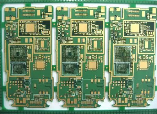
Currently, the PCB surface treatment processes used by domestic manufacturers include: Hot Air Solder Leveling (HASL), immersion tin, immersion silver, OSP (Organic Solderability Preservative), Electroless Nickel Immersion Gold (ENIG), and electroplated gold, among others. Of course, there are also some special PCB surface treatment processes for specific applications.
Comparing different PCB surface treatment processes, their costs vary, and their applications differ. The goal is to choose the right one rather than the most expensive. There is currently no perfect PCB surface treatment process suitable for all application scenarios (this refers to cost-effectiveness, meaning the lowest price that meets all PCB application scenarios). This is why there are so many processes available for us to choose from. Each process has its own merits, and their existence is justified; the key is to understand and utilize them effectively.
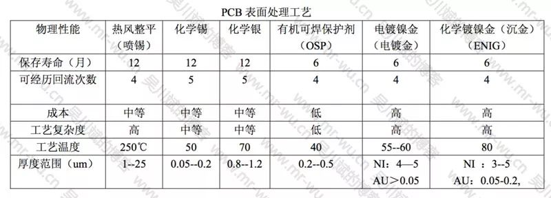
Next, let’s compare the advantages, disadvantages, and applicable scenarios of different PCB surface treatment processes.
Bare Copper Board
-
Advantages: Low cost, smooth surface, good solderability (if not oxidized).
-
Disadvantages: Easily affected by acid and humidity, cannot be stored for long; must be used within 2 hours after unsealing, as copper exposed to air easily oxidizes; cannot be used for double-sided boards, as the second side will oxidize after the first reflow soldering. If there are test points, solder paste must be applied to prevent oxidation; otherwise, it will not make good contact with the probe later.
Hot Air Solder Leveling (HASL)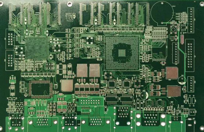
-
Advantages: Relatively low price, good soldering performance.
-
Disadvantages: Not suitable for soldering fine-pitch pins and very small components due to poor surface flatness. Solder beads can easily form during PCB processing, which can cause short circuits for fine-pitch components. When used in double-sided SMT processes, the second side, having undergone high-temperature reflow soldering, is prone to re-melting of the solder, leading to solder beads or droplet-like solder points due to gravity, resulting in an uneven surface that affects soldering quality.
The HASL process used to dominate PCB surface treatment processes. In the 1980s, over three-quarters of PCBs used HASL, but its usage has been declining over the past decade. The HASL process is relatively dirty, unpleasant, and hazardous, making it less favored. However, it is excellent for larger components and wider spacing. In high-density PCBs, the flatness of the HASL process affects subsequent assembly; thus, HDI boards generally do not use HASL. With technological advancements, there are now HASL processes suitable for assembling smaller pitch QFP and BGA components, but actual applications are limited. Currently, some factories are using OSP and immersion gold processes to replace HASL; technological developments have also led some factories to adopt immersion tin and immersion silver processes. Additionally, the trend towards lead-free processes has further restricted the use of HASL. Although there are now so-called lead-free HASL processes, they may involve compatibility issues with equipment.
OSP (Organic Solderability Preservative)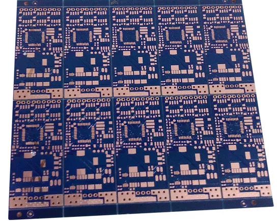
-
Advantages: Retains all the advantages of bare copper boards; boards that have expired (three months) can be re-treated, but usually only once.
-
Disadvantages: Easily affected by acid and humidity. When used for secondary reflow soldering, it must be completed within a certain time; typically, the effect of the second reflow soldering is poorer. If stored for more than three months, it must be re-treated. After opening the package, it must be used within 24 hours. OSP is an insulating layer, so solder paste must be applied to the test points to remove the original OSP layer for electrical testing.
OSP can be used for low-technology PCBs as well as high-technology PCBs, such as single-sided TV PCBs and high-density chip packaging boards. OSP is also widely used for BGA applications. If the PCB does not have functional requirements for surface connections or storage period limitations, OSP will be the ideal surface treatment process. However, OSP is not suitable for low-volume, diverse products, nor for products with uncertain demand forecasts. If a company’s PCB inventory often exceeds six months, it is really not recommended to use OSP-treated boards.
Electroless Nickel Immersion Gold (ENIG)
-
Advantages: Not easily oxidized, can be stored for long periods, smooth surface, suitable for soldering fine-pitch pins and small components. It is the preferred choice for key PCBs. It can undergo multiple reflow soldering without significantly reducing solderability. It can be used as a substrate for Chip On Board (COB) wire bonding.
-
Disadvantages: Higher cost, poorer soldering strength due to the use of electroless nickel plating, which can lead to black pad issues. The nickel layer can oxidize over time, raising long-term reliability concerns.
ENIG differs from OSP in that it is mainly used for boards with functional requirements for surface connections and longer storage periods, such as key contact areas, edge connection areas of router housings, and electrical contact areas for flexible connections of chip processors. Due to the flatness issues of HASL and the cleaning issues of OSP flux, ENIG was widely used in the 1990s; however, its application has decreased due to the emergence of black pad and brittle nickel-phosphorus alloy issues. Nevertheless, almost every high-tech PCB factory now has an ENIG line. Considering that solder joints can become brittle when removing copper-tin intermetallic compounds, issues can arise at the relatively brittle nickel-tin intermetallic compound. Therefore, portable electronic products (such as mobile phones) almost exclusively use OSP, immersion silver, or immersion tin to form copper-tin intermetallic compound solder joints, while ENIG is used for key areas, contact areas, and EMI shielding areas, known as selective ENIG processes.
Immersion Silver (ENIG)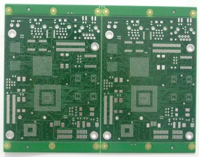 Immersion silver is cheaper than immersion gold. If the PCB has functional connection requirements and needs to reduce costs, immersion silver is a good choice. With its good flatness and contact properties, immersion silver should be chosen. It is widely used in communication products, automotive applications, and computer peripherals, and it is also used in high-speed signal designs. EMS recommends using immersion silver because it is easy to assemble and has good inspectability. However, due to defects such as loss of luster and solder voids, its growth has been slow (but not declining).
Immersion Tin (ENIG)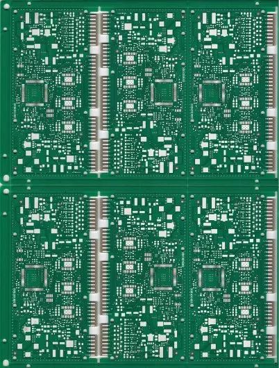
Immersion tin was introduced as a surface treatment process in the last decade, resulting from the demands of production automation. Immersion tin does not introduce any new elements at the soldering points, making it particularly suitable for communication backplanes. Beyond the storage period, tin will lose solderability, so immersion tin requires good storage conditions. Additionally, the use of carcinogenic substances in the immersion tin process has led to restrictions on its use.
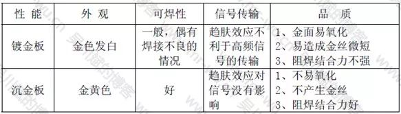
Old Wu often finds that friends are confused between immersion gold and gold plating processes. Below, we will compare the differences and applicable scenarios between immersion gold and gold plating processes.
-
Immersion gold and gold plating form different crystal structures; immersion gold boards are easier to solder than gold-plated boards, preventing soldering defects;
-
Immersion gold boards only have nickel-gold on the pads, and the skin effect in signal transmission occurs in the copper layer, which does not affect the signal;
-
Immersion gold has a denser crystal structure than gold plating, making it less prone to oxidation;
-
Immersion gold boards only have nickel-gold on the pads, preventing gold wire from causing micro-short circuits;
-
Immersion gold boards only have nickel-gold on the pads, ensuring a stronger bond between the solder mask and copper layer;
-
Immersion gold appears golden yellow, which is more aesthetically pleasing than gold plating;
-
Immersion gold is softer than gold plating, so it is less durable; for gold finger boards, gold plating is more effective.