Today, I will share with you the 8 common PCB markings found on PCB boards.
From left to right: Stamping hole – Via type – Solder mask pad – Reference mark
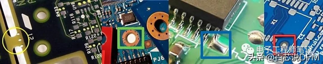
From left to right: Stamping hole – Mounting hole – Solder mask pad – Reference mark
From left to right: PCB slot, PCB button, spark gap, and fuse trace
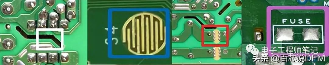
From left to right: PCB slot, PCB button, spark gap, and fuse trace
1. PCB Stamping Hole
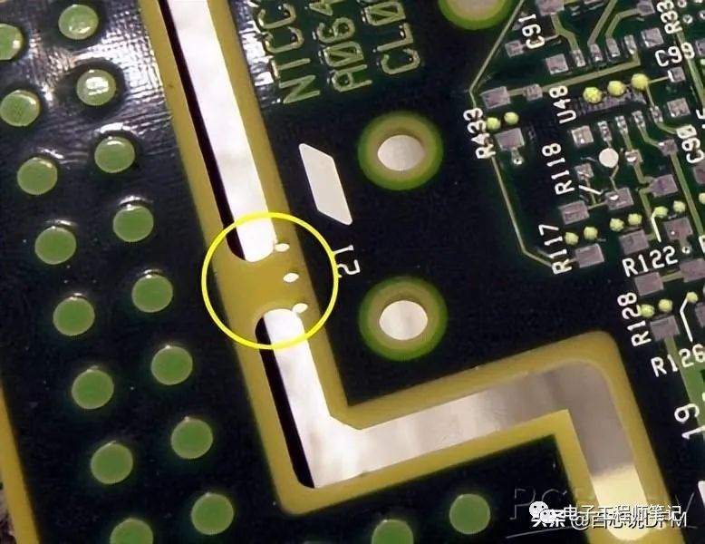
Stamping hole
When assembling boards, in order to facilitate separating the PCB board, a small contact area is reserved in the middle, and the holes in that area are called stamping holes. I personally think the reason for naming it a stamping hole is that when the PCB is separated, it leaves an edge like a postage stamp.
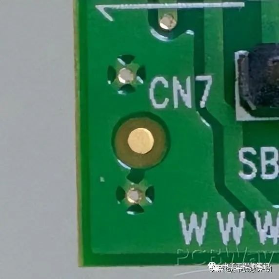
2. PCB Via Type
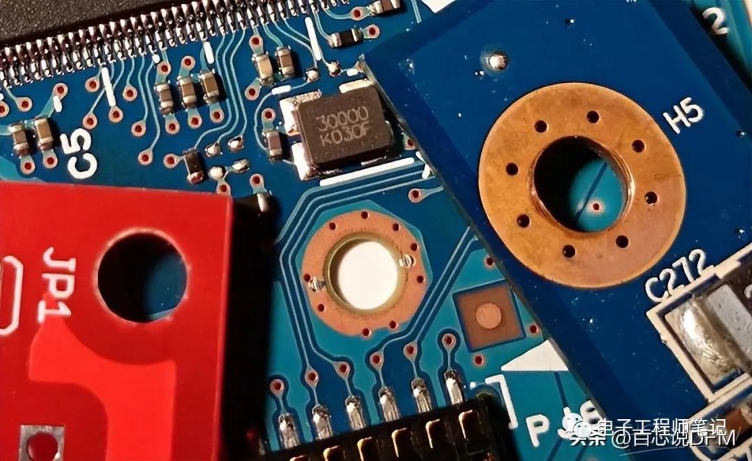
PCB via type
In many cases, you will see mounting holes surrounded by small vias. There are mainly 2 types of mounting holes: plated and non-plated. There may be 2 reasons for using the surrounding vias:
-
1. When we want to connect the hole to the inner layer (such as GND in multilayer PCBs)
-
2. In the case of non-plated holes, when wanting to connect the upper and lower pads
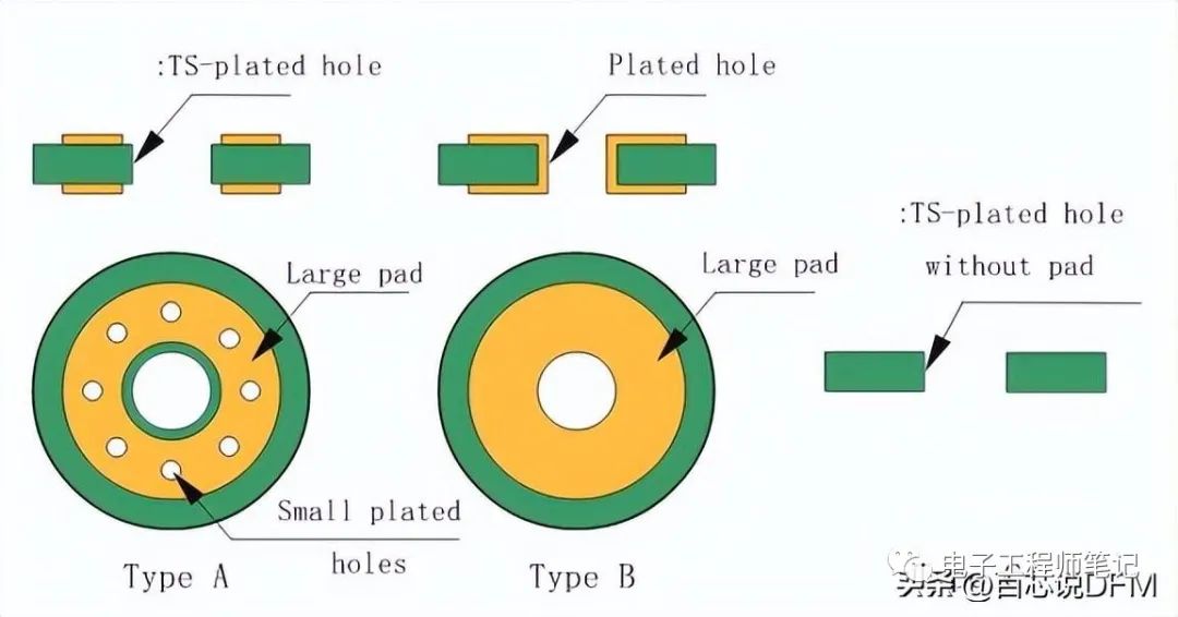
3. Solder Mask Pad (Solder Theft)
One of the defects of wave soldering is that solder bridges can easily occur during the SMD soldering process. As a solution, it was found that using an additional pad at the end of the original pin can solve this problem. The width of the additional pad is 2-3 times that of the normal pad.
It is also known as solder theft, as it absorbs excess solder and prevents solder bridges.

Solder mask pad
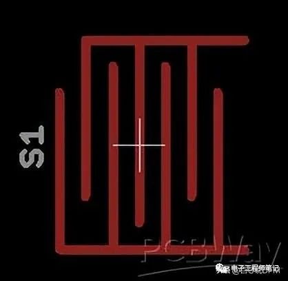
4. Reference Mark (Mark Point Mark)
Reference mark
A larger bare circle contains a bare copper circle. This reference mark is used as a reference point for pick-and-place (PnP) machines. The reference mark is located in three positions:
-
1. In the panel.
-
2. Next to small pitch components such as QFN, TQFP, etc.
-
3. At the corners of the PCB.
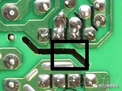
5. Spark Gap
The spark gap is used for ESD, current surge, and overvoltage protection. High voltage can ionize the air between two terminals, and a spark will form between them before damaging the rest of the circuit. This type of protection is not recommended, but it is better than having none; the main drawback is that the performance changes over time.
The breakdown voltage can be calculated using the following formula: V=((3000×p×d)+1350)
Where “p” is the atmospheric pressure and “d” is the distance in millimeters.
Spark gap
6. PCB Conductive Button
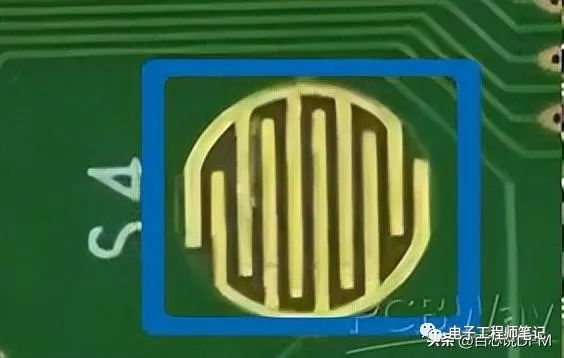
PCB conductive button
If you have ever disassembled a remote control or calculator, you should have seen this marking. Conductive buttons consist of 2 interleaved terminals (but not connected). When the rubber button on the keyboard is pressed, the two terminals connect because the bottom of the rubber button is conductive.
PCB conductive button
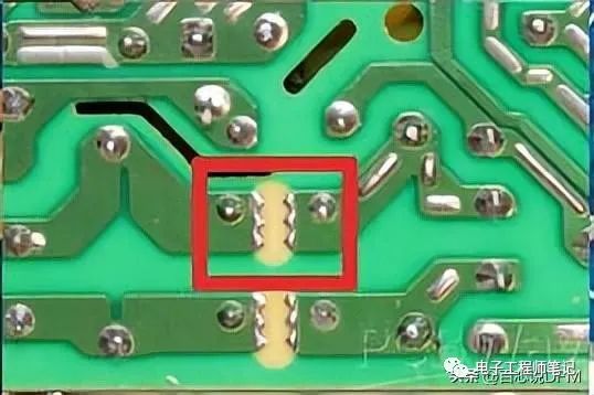
7. Fuse Trace
Similar to the spark gap, this is another cheap technology using PCB. Fuse traces are necked traces on the power line, acting as one-time fuses. The same configuration can be used as PCB jumpers by simply etching the necked trace to remove specific connections (PCB jumpers can be found on some Arduino UNO boards on reset lines).
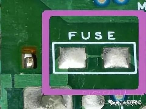
Fuse trace
8. PCB Slot
If you look at high-voltage devices like power supplies, you may notice gas slots between certain traces.
Temporary arcs that repeatedly occur in PCBs can lead to carbonization of the PCB, resulting in short circuits. To address this, routing slots can be added in suspected areas, which will still experience arcing but will not carbonize.
PCB slot
Disclaimer: The copyright of this article belongs to the original author and does not represent the views of the association. The articles pushed by the “Jiangxi Province Electronic Circuit Industry Association” are only for sharing purposes and do not represent the position of this account. If there are copyright issues, please contact us for deletion.