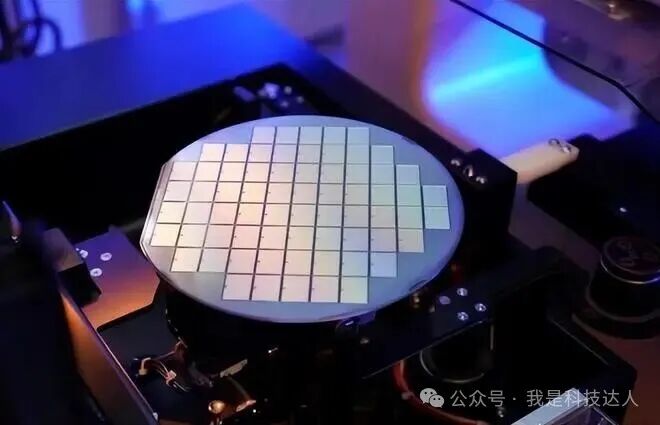
Recently, significant news has emerged from Wuhan’s Optics Valley—the first domestic 12-inch silicon photonic chip wafer platform based on 40nm CMOS technology has officially been put into operation. This platform, led by the National Information Optoelectronics Innovation Center (NOEIC), achieves full autonomy in process design, testing, and packaging, marking a critical transition for China’s silicon photonic industry from ‘single-point breakthroughs’ to ‘scale autonomy’. This development breaks the long-standing foreign monopoly on technology and production capacity, injecting core momentum into the high-quality development of the digital economy.

1. Technical Features: Photonic Transmission + Domestic Closed Loop, Defining a New Benchmark for Efficient Chips
Silicon photonic chips use photons as information carriers, offering revolutionary advantages over traditional electronic chips: transmission rates increase by more than 10 times, and power consumption decreases by 30%. This is akin to upgrading from ‘road transport’ to ‘light-speed high-speed rail’, perfectly adapting to the high-frequency demands of AI large models, cloud computing, and other scenarios. The core highlights of the newly launched 12-inch platform are prominent, with key indicators reaching internationally advanced levels.
In terms of the process system, the platform achieves full domestic production of three core kits: PDK (Process Design Kit), TDK (Test Design Kit), and ADK (Assembly Design Kit), establishing autonomous technical standards that meet domestic industrial needs, completely eliminating dependence on foreign technology. In terms of production efficiency, the usable area of 12-inch wafers increases the number of chips per wafer by 2.38 times compared to 8-inch wafers, and combined with process optimization, significantly improves yield, reducing unit chip costs by about 30%, with initial signs of scale effects. More innovatively, the platform adopts an MPW (Multi-Project Wafer) shared service model, integrating multiple compatible designs into a single wafer run, reducing the cost of a single R&D project from millions to hundreds of thousands, greatly lowering the innovation threshold for the industry.

2. R&D Challenges: Breaking Through Multiple Barriers to Build an Autonomous Industrial Ecosystem
The successful launch of the 12-inch silicon photonic wafer platform is the result of overcoming multiple technical barriers. Previously, China’s silicon photonic industry faced a ‘bottleneck’ dilemma: core design kits were monopolized by foreign entities, wafer runs required high licensing fees and faced supply risks; the production capacity of platforms smaller than 8 inches was limited, with significant edge losses, making it difficult to achieve scale effects; and the integration of optoelectronic and microelectronic processes posed high challenges, with key indicators such as waveguide loss control and optical coupling efficiency being difficult to overcome.
The R&D team has spent a long time tackling these issues, not only solving the compatibility problem of photons and electrons working together on silicon-based materials but also achieving stability and repeatability control throughout the entire process, shortening the wafer run cycle from the traditional 6-8 months to 3-4 months, effectively doubling the R&D iteration efficiency. As the second 12-inch silicon photonic mass production platform globally after the United States, this breakthrough fills a domestic technological gap, proving that China has mastered the core technologies of silicon photonic chips from design, manufacturing to testing and packaging, possessing the hard power to build an autonomous industrial ecosystem.

3. Social Applications: Empowering Upgrades Across Multiple Fields, Activating New Momentum for the Digital Economy
The large-scale application of silicon photonic chips will trigger transformations in several key areas. In the computing infrastructure sector, it can provide high-speed, low-power data transmission support for AI large model training and cloud computing centers, enhancing the efficiency of China’s computing network; in the communications sector, it adapts to the needs of 5G upgrades and 6G R&D, promoting the construction of ultra-high-speed communication networks and solidifying the foundation of digital infrastructure.
At the industrial application level, the platform has already supported Huagong Technology in completing small-batch trial production of 3.2T optical module chips, achieving industrialization verification of technological results through compatibility testing with mainstream manufacturers. In the future, as costs continue to decrease, silicon photonic technology will extend from high-end scenarios to civilian fields, opening up vast application spaces in smart terminals, industrial internet, and high-end manufacturing. According to industry forecasts, by 2030, the market share of silicon photonic chips in the optical communication chip market is expected to surge to 60%, with the market size likely to exceed $10 billion, and the platform’s launch will help China seize the high ground in the global optoelectronics industry.
The launch of the 12-inch silicon photonic wafer platform is another milestone breakthrough for China’s Optics Valley in the field of optoelectronics, demonstrating the strategic wisdom of China in differentiating itself in the chip industry. As the platform continues to empower innovative entities, it will attract more talent and capital into the sector, nurturing a vibrant silicon photonic industry ecosystem. In the future, China’s silicon photonic industry is expected to form a virtuous cycle of ‘technology iteration—scale expansion—cost optimization’, providing solid support for building a strong technological nation and securing a favorable position in the new round of global technological revolution.