The CPU has developed over the past 40 years, and this year, Intel has launched the 8086K CPU commemorative edition to celebrate the 40th anniversary of the first 8086 CPU. The CPU bus has also undergone many generations of evolution. Taking Intel as an example, the CPU bus has evolved from FSB to QPI, while AMD transitioned from FSB to HT LINK, leading to the current GMI bus. Today, let’s take a look at these buses.
1: FSB (Front Side Bus)
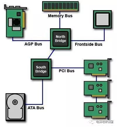
Friends familiar with computers know that older motherboards had separate north and south bridges. For the CPU to communicate with memory, it had to go through the north bridge, i.e., CPU-north bridge-memory. This communication bus is the FSB. In the early days, the CPU’s external frequency was synchronized with the FSB frequency. That is, external frequency = FSB frequency. For example, the external frequency of the Celeron 300A was 66MHz, so its FSB frequency was also 66MHz. However, by the time of the Pentium 4, the FSB bus speed could no longer meet the bandwidth requirements of the CPU, so Intel introduced Quad Pumped Bus technology, allowing the FSB to transmit four times the data in one cycle. This is the calculation method we are most familiar with: FSB frequency = external frequency x 4. For instance, a CPU with an external frequency of 333MHz has an FSB frequency of 1333MHz, greatly expanding the transmission speed between the CPU and the north bridge. Initially, FSB was not only used for communication between the CPU and the north bridge; Intel’s early dual-core processors also used the FSB bus for data exchange. Intel simply packaged two dies into one chip, so communication between CPUs had to go through the north bridge. Early AMD processors also used the FSB bus.
2: HT LINK
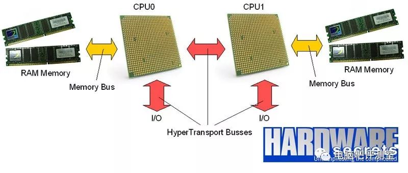
This bus structure was first proposed by AMD in the K8 processor and is also known as HyperTransport. AMD introduced it in 1999, and later, major players like NV, ATI, and IBM supported it. The HT bus technology is open to the public, with improvements made by the alliance’s major players. The HT bus has a terrifying transmission rate. The first version, 1.0, was released in 2001, achieving a maximum bidirectional transmission rate of 12.8GB/s, although AMD’s single-channel 16-bit implementation did not reach this speed. At the same time, Intel was still using the FSB bus, which had a transmission bandwidth of only 4.3GB/s at 533MHz. The HT bus has multiple versions, with the final HT3.1 bus released in 2008, achieving a maximum bandwidth of 51.2GB/s. This figure is still impressive even today. The HT bus is not only used for communication with memory; it is also used among AMD’s multi-CPU setups. Cisco has even implemented the HT bus in routers and switches, greatly enhancing the multi-path transmission capabilities of switches. AMD was also one of the first manufacturers to integrate the memory controller into the CPU.
3: QPI LINK
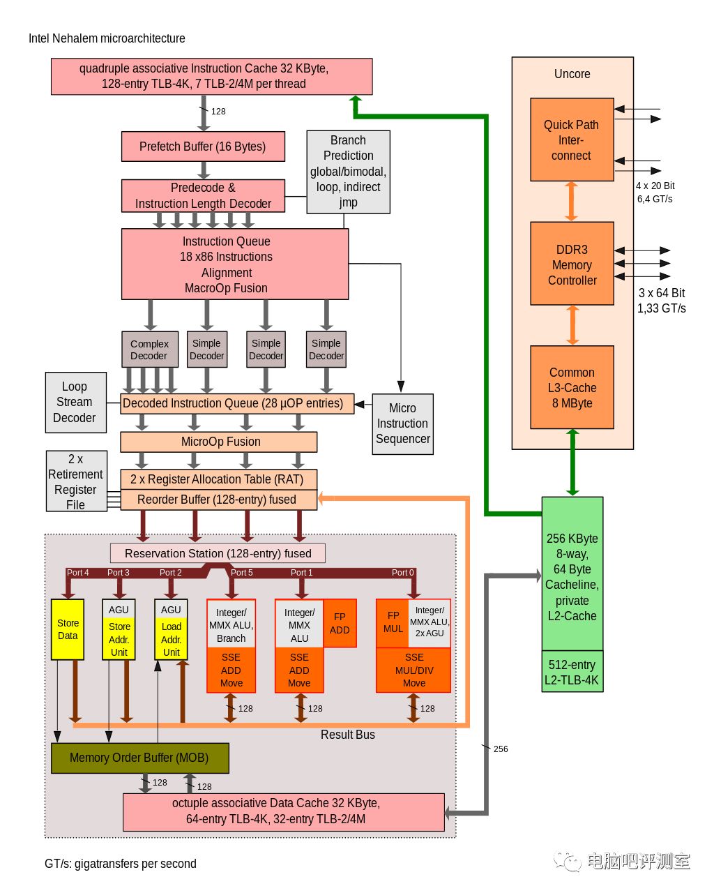
QPI stands for Quick Path Interconnect. In fact, the QPI bus was already used in Itanium and Xeon platforms to replace the outdated FSB. It was introduced to the desktop level starting with the first generation Nehalem processors. Up to today, all CPUs, including the 8700K, are based on the QPI bus for communication. Like HT LINK, the QPI bus is also a point-to-point communication system used for direct connections between the CPU, north bridge, and south bridge. Its speed far exceeds that of the FSB bus; for instance, with the last generation’s 1600MHz FSB, the transmission speed is 12.8GB/s, while the initial QPI bus achieved a speed of 25.6GB/s, effectively doubling the previous generation’s speed. With the introduction of the SNB architecture, the bus with the integrated CPU memory controller still derives from the QPI bus, but due to its ring topology, it greatly enhances speed while maintaining cache coherence. Communication with the south bridge has always used the DMI bus.
4: Infinity Fabric
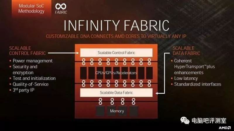
The first time I heard about this new bus, it was referred to as the GMI bus in the news, but it was officially named Infinity Fabric in AMD’s ZEN processor release presentation, and we often call it the CCX bus. Infinity Fabric is not a complex concept; it is derived from the HT bus. However, compared to the open HT bus technology, Infinity Fabric is AMD’s proprietary technology, and if you want to use it, you must pay a licensing fee. Infinity Fabric can be considered the cornerstone of AMD in this era, with transmission rates ranging from 30GB/s to 512GB/s, and it is not compatible with the HT bus. Infinity Fabric is divided into SCF and SDF. SDF is responsible for data transmission, while SCF handles control transmission commands. The SDF part is derived from the HT bus. Like the HT bus, Infinity Fabric is not limited to CPUs; it can also be used for GPUs and APUs, although their SDF layers differ. However, in the latest APUs, the connection between the CPU and GPU still uses the PCI-E bus, and we have not seen the CCX bus; perhaps this generation of APUs is merely a rushed product from AMD, and we hope to see a complete APU in the next generation.
It must be said that with the development of computers, the bus technology has also continuously evolved. From the outdated FSB to high-speed buses like HT and QPI, what kind of monstrous buses will we see in the future? After all, compared to AMD’s Infinity Fabric, the speed of QPI is indeed hard to look at. However, any bus replacement or iteration will have to wait for a new architecture. We look forward to new surprises from AMD and Intel next year.
If you liked this article,
feel free to give it a thumbs up,
leave a comment below,
or follow the Computer Bar Review Room’s WeChat public account, a self-media platform.

You are also welcome to join the official QQ group of the Computer Bar Review Room: 201801391.
You can also follow Bilibili @翼王 or Weibo @渐缜_脑吧, @DDAA117, @我家智天用win8!