1. Company Overview of Jingyuda
In the past, this process was tightly controlled by international giants: expensive equipment, closed processes, and long lead times for spare parts, often leading to “production line waiting for parts.” Now, in response to the domestic substitution demand for semiconductor equipment and the low domestic rate, a group of semiconductor industry experts has gathered in Zhuji, Zhejiang, a land famous for its pearls, supported by Zhejiang Huawai Holdings and Wan’an Group, to establish “Zhuji Jingyuda Semiconductor Technology Co., Ltd.” The company’s goal is singular: to achieve “100% domestic parts + open-source processes” for semiconductor equipment that is currently low in domestic production and constrained. This will allow customers to achieve “zero cost for line change.” Therefore, Jingyuda will invest substantial resources in the development and production of Chemical Mechanical Polishing (CMP) equipment, Reactive Ion Etching (RIE-ICP) equipment, and Atomic Layer Deposition (ALD) equipment.
Jingyuda’s first CMP equipment has completed testing and is about to be deployed for 8-12 inch silicon wafers in the 14/7/5 nm chip process, thinning wafers for advanced CoWoS packaging to below 35 microns, manufacturing 6-8 inch silicon carbide (SiC) wafers and power chips, as well as wafer production. The company fully controls three core technologies:
Core Technologies① 100%Domestic Parts+Open-Source Processes
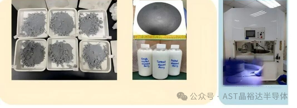
For the polishing pads and slurries, our team has mastered a 100% self-made core formula and synthesis technology, allowing for “one-click formulation” based on customer wafer material. The entire process menu is open-source, enabling FAB engineers to modify parameters themselves, no longer constrained by overseas “black boxes.”
Core Technologies
② Innovative Polishing Technology
The core of this technology lies in combining “optical composite abrasives,” “laser/plasma assistance,” and “immersion polishing mechanisms,” which disrupts the traditional concepts of purely mechanical or chemical mechanical polishing (CMP).
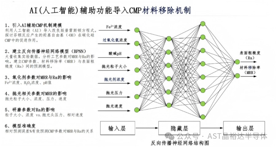
Core Technologies③ AIProcess Migration
Jingyuda has built-in self-developed AI Pilot models, allowing customers to run just 20 “learning wafers,” after which the system can migrate old line processes to new lines, automatically matching formulations and achieving a production yield of ≥98%. This results in “zero cost for customers to change lines.”
2. Performance of Our CMP Equipment
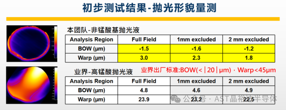
Through our technical production tests, we have achieved uniform, efficient, and damage-free modification of silicon carbide (SiC) substrate surfaces, resulting in surface quality, uniformity, and environmental friendliness far exceeding traditional methods. The comparative data is shown in the table below.

Recycled Wafer Production Line
Our advantage is “more advanced technology” and “better understanding of recycling”—treating wafer recycling as an independent industry rather than an “ancillary process” of FAB. This creates a “dislocated competitive advantage” over domestic high-end CMP manufacturers in terms of cost, efficiency, service, and trust.

3. Future Plans
To further refine CMP technology, we will develop plasma technology, which is also the foundation for RIE-ICP and ALD equipment. Our team will first apply plasma technology to CMP equipment, which will aid in achieving 1 nm process technology. The characteristics of using plasma technology in CMP equipment are as follows:
Non-contact mechanical polishing, elimination of subsurface damage, no water discharge, environmentally friendly, no polishing pads or slurries, recoverable value of discharged gases (carbon credit trading), high etching rates for thinning, low etching rates for polishing, reduced thinning and polishing costs and time, and reduced breakage risk, improved yield, stress release, and reduced warpage.
Domestic chip production has never been just a slogan, but a series of counterattacks after being “choked”.
Jingyuda aims to be the sharpest “Zhuji pearl,” completely grinding down the last overseas barrier in thinning and CMP!
END –
Written by | Jingyuda Marketing Department
©2025 Jingyuda Semiconductor All Rights Reserved