The rules of WeChat have been adjusted.
I hope everyone can click ‘View’ and ‘Like’ more after reading the article, and if you like it, please share it.
This way, the push notifications from Chip Driver can continue to appear in your subscription list.
We can continue to share high-quality content in the integrated circuit design industry with everyone~
Source: Content from http://www.cnblogs.com/IClearner/ , Author: IC_learner, thank you.
Previously, we discussed optimization methods for gate-level power consumption, including static, dynamic, and total power consumption. Now, let’s document a commonly used low-power method at the gate level (which some books also refer to as system level) — Power Gating.
① Overview and Principle of Power Gating
Power gating refers to the disconnection of the power supply to a certain area of the chip, meaning that the power supply to the logic circuits within that area is turned off. The design of power gating (Power Gating) is shown in the figure below:
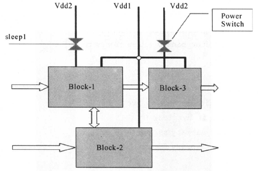
If a certain module is not working for a period of time, its power supply can be turned off (the power supply can be turned off using an MTCMOS switch, which is typically added during the backend layout and routing process; this belongs to backend knowledge and will not be introduced here). After power is cut off, the design enters a sleep mode with very low leakage power. Upon waking up, in order for the module to quickly return to working mode, it is necessary to maintain the state before power was cut off. A retention register can be used to remember the state. The design of power gating using a retention register is shown in the figure below:
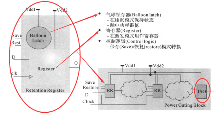
Now let’s explain the design above:
-
In sleep mode, the power supply Vdd2 of the register is cut off, so its leakage power is extremely low; at this time, only the latch is kept in working state, and the value of the register is retained in the latch. Since the latch is composed of transistors with high threshold voltage, the leakage power is very low.
-
When the Restore signal is activated, the power supply Vdd2 of the register is applied, and the value retained in the latch is loaded into the register. When the register is in working (active) state, it operates as a general register. The Save/Restore pins are also referred to as power gating pins; they are used to place the circuit in the appropriate mode.
-
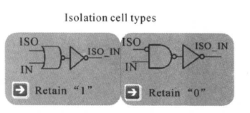
The output of the power gating module needs to use an isolation cell (we discussed this earlier), because during sleep mode, the output of the module is an uncertain value. To ensure that the input of the next stage does not float during sleep mode, an isolation cell is inserted to provide an output of “1” or “0”, ensuring that the input of the next stage has a definite logical value, as shown below:
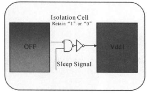
ISO is the sleep control signal used to control the operation of the isolation cell. When the circuit is in normal working mode, ISO=0, ISO_IN=IN. In sleep mode, when ISO=1, if the unit shown in the left figure below is used as the isolation cell, the output logic is “1”; if the unit shown in the right figure below is used as the isolation cell, the output logic is “0”:
② Power Gating Cells in the Technology Library
To carry out power gating design, support from the synthesis library is required. The library model of the power gating cells in the synthesis library is shown below:
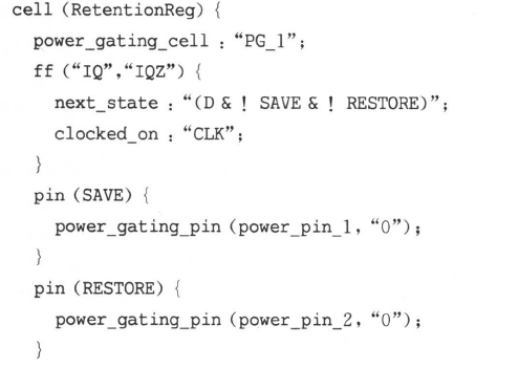
Below is a partial explanation of the library model:
-
Cell level attribute
power_gating_cell:”type”, “type” cannot be “none” or an empty character; it identifies the type of retention register described. In this case, the type of retention register is PG_1.
-
Function description of the power gating register
 It is the function of the retention register in active mode.
 -
Pin level attribute
 power_pin_1~ power_pin_5 lists the names of existing power gating signals. For example, power_pin_1 can be defined as the sleep signal, and power_pin_2 can be defined as the wake signal. The default value of power_pin_[1-5] signals is the value when the register is in a non-working (disable) state, which can be “0” or “1”. For example, if the logical value of power_pin_1 is “1”, the circuit enters sleep mode, then its non-working (disable) value should be logical “0”.
③ Power Gating Design Flow
Having understood the principle of power gating and the power gating cells in the synthesis library, let’s introduce the design flow of power gating. The design flow and corresponding scripts for using power gating are shown below:
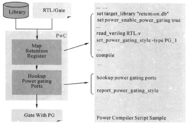
Let’s explain some of the commands:
-
The command set_power_gating_style is used in the script to map the retention register. For the code below:
······
always@ (posedge clk) begin:sub_block_1
g=d;
end
······
the command set_power_gating -style -type PG_1 -hdl_block sub_block_1 can map the registers in the code to retention registers. The option “-type PG_1” specifies using the retention register of type PG_1 from the library. The option “-hdl_block sub_block_1” specifies replacing all registers in the RTL code process named “sub_block_1” with retention registers of type PCG_1.
-
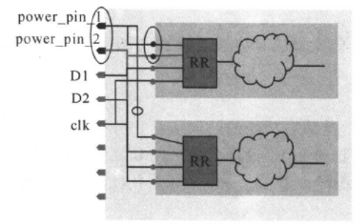
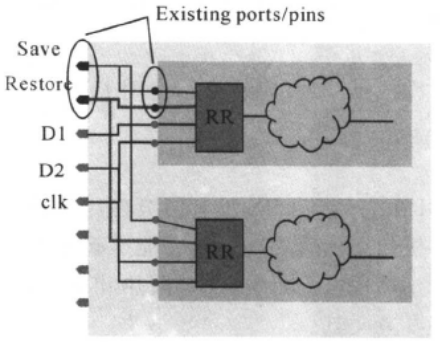
The command hookup_power_gating_ports in the script automatically inserts power_pin[1-5] ports and pins of hierarchical modules. Ports or pins with the same power pin attribute will be connected together. For example, pins with the attribute “power_pin_1” will be connected together, with the default name “power_pin_1”. The figure below shows the ports and pins of hierarchical modules inserted after executing the hookup_power_gating_ports command. We can use the options “-default_port_naming_style” and “-port_naming_styles” to change the naming of ports and/or hierarchical module pins:
The following script uses the command set_power_gating_signal to specify connecting the power gating pins with existing ports or hierarchical pins, as follows:
set_power_gating_signal -power_pin_index 1 [get_ports Save]
set_power_gating_signal -power_pin_index 2 [get_pins A/p1]
······
hookup_power_gating_ports
The results are as follows:
-
Finally, we can use the report_power_gating command to report the power gating units in the design, as shown below: