
Source: Content fromhttp://www.cnblogs.com/IClearner/, Author: IC_learner, Thank you.

Gate Level Circuit Low Power Design Optimization
(1) Overview of Power Optimization for Gate Level Circuits
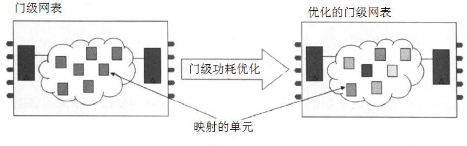
Gate Level Power Optimization (GLPO) starts from the already mapped gate-level netlist, optimizing the design’s power consumption to meet power constraints while maintaining performance, i.e., satisfying design rules and timing requirements. The design before power optimization is already mapped to the technology library, as shown in the figure below:
Power optimization for gate level circuits includes optimizing total power consumption, dynamic power, and leakage power. The priority order for optimization is as follows:
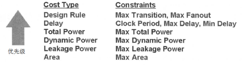
From this, we can see that during optimization, the generated circuit must first meet the design rule requirements, then the delay (timing) constraints. After satisfying timing performance requirements, total power optimization is performed, followed by dynamic power optimization and leakage power optimization, with area optimization last.
During optimization, higher priority constraints must be satisfied first. Optimizing lower priority constraints cannot come at the expense of higher priority constraints. Power optimization cannot degrade the timing of the design. To effectively perform power optimization, there must be positive timing slacks in the design. The reduction in power consumption is exchanged for positive timing slack on timing paths, meaning that power optimization will reduce positive timing slack on timing paths. Therefore, the more positive timing slack there is in the design, the greater the potential to reduce power consumption.
With the above description, we now have an understanding of gate level power optimization. Here, I will first introduce a method for static power optimization—multi-threshold voltage design, followed by dynamic power optimization based on EDA tools, and finally, overall power optimization. I will introduce a commonly used gate level low power method—power gating—tomorrow; today’s content mainly revolves around static, dynamic, and total power.
(2) Multi-Threshold Voltage Design
① Principle of Multi-Threshold Voltage Design
As semiconductor processes advance, the geometric sizes of semiconductor devices are getting smaller, the number of transistors (gates) in devices is increasing, and the supply voltage for devices is decreasing, resulting in lower threshold voltage for unit gates. Due to the increasing number of unit gates per unit area, power density is high, leading to high power consumption in devices. Therefore, during design, we must optimize and manage power consumption. In 90nm processes or below, static power accounts for more than 20% of the total design power consumption. Therefore, when using ultra-deep submicron processes, it is necessary to reduce both dynamic and static power consumption. In ultra-deep submicron processes, the relationship between threshold voltage and leakage power (static power) is shown in the figure below:
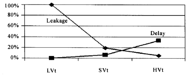
As seen in the figure, the threshold voltage Vt exponentially affects leakage power. The threshold voltage Vt has the following relationship with leakage power and unit gate delay:
For units with a higher threshold voltage Vt, the leakage power is lower, but the gate delay is longer, meaning slower speed;
For units with a lower threshold voltage Vt, the leakage power is higher, but the gate delay is shorter, meaning faster speed.
We can utilize this characteristic of multi-threshold voltage technology libraries to optimize leakage power and design circuits with low static power and high performance.
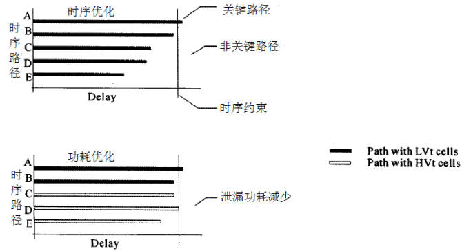
In general designs, a timing path group has multiple timing paths, with the longest delay path referred to as the critical path. Based on the characteristics of multi-threshold voltage units, to meet timing requirements, low threshold voltage cells (low Vt cells) are used in the critical path to reduce unit gate delay and improve path timing. To reduce static power, high threshold voltage cells (high Vt cells) are used in non-critical paths to decrease static power consumption. Therefore, by using a multi-threshold voltage technology library, we can design low static power and high performance designs. The above description is illustrated in the figure below:
② Multi-Threshold Voltage Design for Gate Level Netlist/RTL Code
Multi-threshold voltage design can be performed during gate-level netlist or RTL code generation, or after routing. The process for multi-threshold voltage design at the gate level netlist/RTL code (or static power optimization) is as follows:
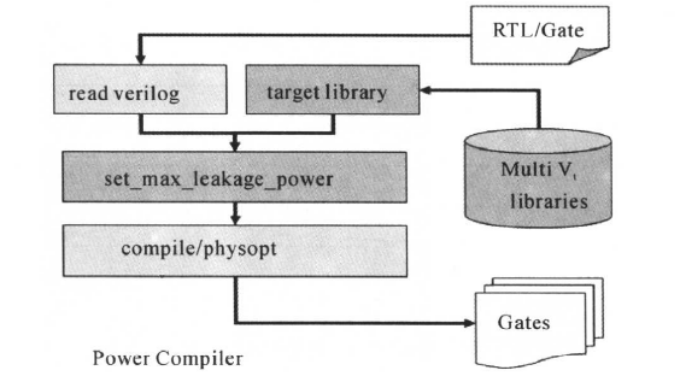
An example script is as follows:
set target_library “hvt.db svt.db lvt.db”
······
read_verilog mydesign.v
current_design top
source myconstraint.tcl
······
set_max_leakage -power 0mw
compile
······
Unlike previous scripts, when setting target_library, we used multiple libraries. In the above, the target library is set to “hvt.db svt.db lvt.db”. The script uses the set_max_leakage_power command to set the static power constraint for the circuit. When running the compile command, Power Compiler will choose suitable units from the target library based on timing and static power constraints, aiming to use Svt or Hvt units as much as possible while satisfying timing constraints, resulting in high performance and low static power in the optimized design.
PS: If performing leakage power optimization in the Physical Compiler tool (currently we use the DC topology mode), we can retain some positive timing slack to prevent the circuit from operating at the limit of timing. These timing slack amounts can also be utilized by other optimization algorithms later. The command to set timing slack is as follows:
set physopt_power_critical_range timing_amount
③ Multi-Threshold Voltage Design After Routing
The above discusses multi-threshold voltage design for gate-level netlist/RTL code; below is a brief introduction to multi-threshold voltage design after routing, as shown in the flow diagram below:
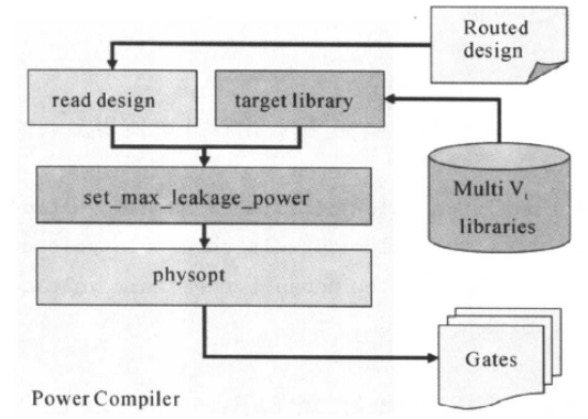
An example script is as follows:
set target_library “hvt.db svt.db lvt.db”
read_verilog routed_design.v
current_design top
source top.sdc
······
set_max_leakage -power 0mw
physopt -preserve_footprint -only_power_recovery -post_route -incremental
The physopt command uses the “-post_route” option specifically for performing leakage power optimization after routing. During optimization, the unit’s footprint is preserved, and the original routing remains unchanged.
④ Report on Multi-Threshold Voltage Design and Multi-Threshold Library
During leakage power optimization, Power Compiler will report the following leakage optimization information:
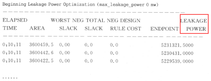
The LEAKAGE POWER column shows the internal optimized leakage cost values. It may differ from the reported leakage power. We use the “report_power” command to obtain an accurate report on power consumption.
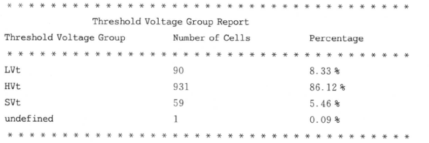
Now let’s take a look at the multi-threshold library.
The multi-threshold library defines two attributes: one for the library attribute: default_threshold_voltage_group, and another for individual library unit attributes: threshold_voltage_group. The command to report the multi-threshold voltage group is: report_threshold_voltage_group. We can use these two attributes of the multi-threshold library to report the proportion of multi-domain value library units used in the design. An example script is as follows:
set_attr -type string lvt.db:slow default_threshold_voltage_group LVt
set_attr -type string svt.db:slow default_threshold_voltage_group SVt
set_attr -type string hvt.db:slow default_threshold_voltage-group HVt
report_threshold_voltage_group
The results of the report are as follows:
(3) Dynamic Power Optimization Based on EDA Tools
After introducing static power optimization, we will now discuss dynamic power optimization. Dynamic power optimization is typically performed after timing optimization is completed. During dynamic power optimization, the circuit’s switching behavior must be provided, and the tools optimize the entire circuit’s dynamic power based on the flip rate of each node. The compile/physopt command can optimize both timing and power simultaneously. The command for setting dynamic power is:
set_max_dynamic_power xxmw. (Generally set to 0)
The dynamic power optimization process is as follows:
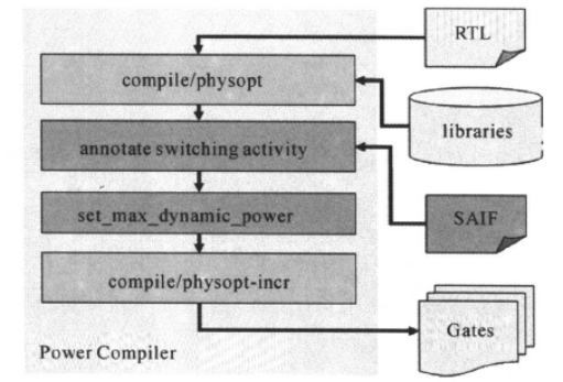
An example script is as follows:
read_verilog top.v
source constraints.tcl
set target_library “tech.db”
compile
read_saif
set_ max_dynamic_power 0 mw
compile -inc
The implementation of dynamic power optimization is as described above. The optimization process utilizes many techniques such as inserting buffers and phase allocation. Since these are automatically implemented by the power compiler (or the principles used by the tool during low power optimization), we will not delve into them here.
(4) Overall Power Optimization
Having introduced methods for static and dynamic power optimization, we can combine them for overall design power optimization. Overall power is the sum of dynamic power and static power, and the priority of overall power optimization is higher than that of dynamic and static power. During overall power optimization, tools aim to minimize the sum of dynamic and static power. If reducing leakage power increases dynamic power, but their sum decreases, the optimization is effective. The opposite is also true. We can set switches to optimize dynamic and static power with different effort levels and weights.
The overall power optimization process is shown in the diagram below:
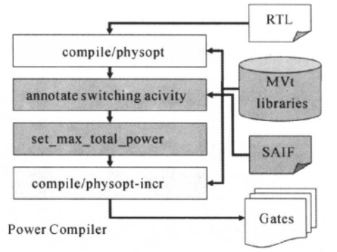
An example script is as follows:
read_verilog top.v
source constraints.tcl
set target_library “hvt.db svt.db lvt.db”
······
compile
read_saif
set_max_total_power 0 mw -leakage_weight 30
compile -inc
In the script, target_library is set to the multi-threshold voltage library for static power optimization. The saif file containing switching behavior is read in to constrain dynamic power optimization. When setting constraints for total power, we can use static or dynamic power weight options in the set_max_total_power command, allowing the tool to prioritize static or dynamic power during optimization. Assuming P, Pd, and Pl represent total power, dynamic power, and static power, and Wd and Wl represent the weights for dynamic and static power, then:
Total power P = (Wd*Pd+Wl*P1)/Wd
We can set the DC or PC to optimize only for power consumption. In this case, the tool only optimizes the power consumption of the design without making any optimizations or corrections to higher priority constraints or causing DRC violations. However, this optimization will not worsen the performance of higher priority constraints or cause DRC violations. The advantage of this optimization is that it has a shorter runtime and can be used to optimize dynamic power, static power, and total power. In DC and PC, it can only work in incremental editing mode.
The command for optimizing only power consumption in PC is as follows:
set_max_total -power 0 mw
physopt -only_power_recovery
The command for optimizing only power consumption in DC is as follows (since PC is now in DC, the script below is more commonly used):
set compile_power_opto_only true
set_max_leakage_power 0 mw
compile -inc